
Adaptive voltage control for SRAM

a voltage control and adaptive technology, applied in the field of integrated circuit design, can solve the problems of limiting the range of operating parameters (e.g., snm and/or vtrip) of the sram cell incurred from the global variation of the circuit elements, and the minimum operating voltage vmin for a chip with a low vtn might be limited by the snm requirements, so as to maintain functionality and performance, reduce power, and spread the characteristics of th

Active Publication Date: 2009-01-29
TEXAS INSTR INC
View PDF16 Cites 14 Cited by
  • Summary
  • Abstract
  • Description
  • Claims
  • Application Information

AI Technical Summary

Benefits of technology

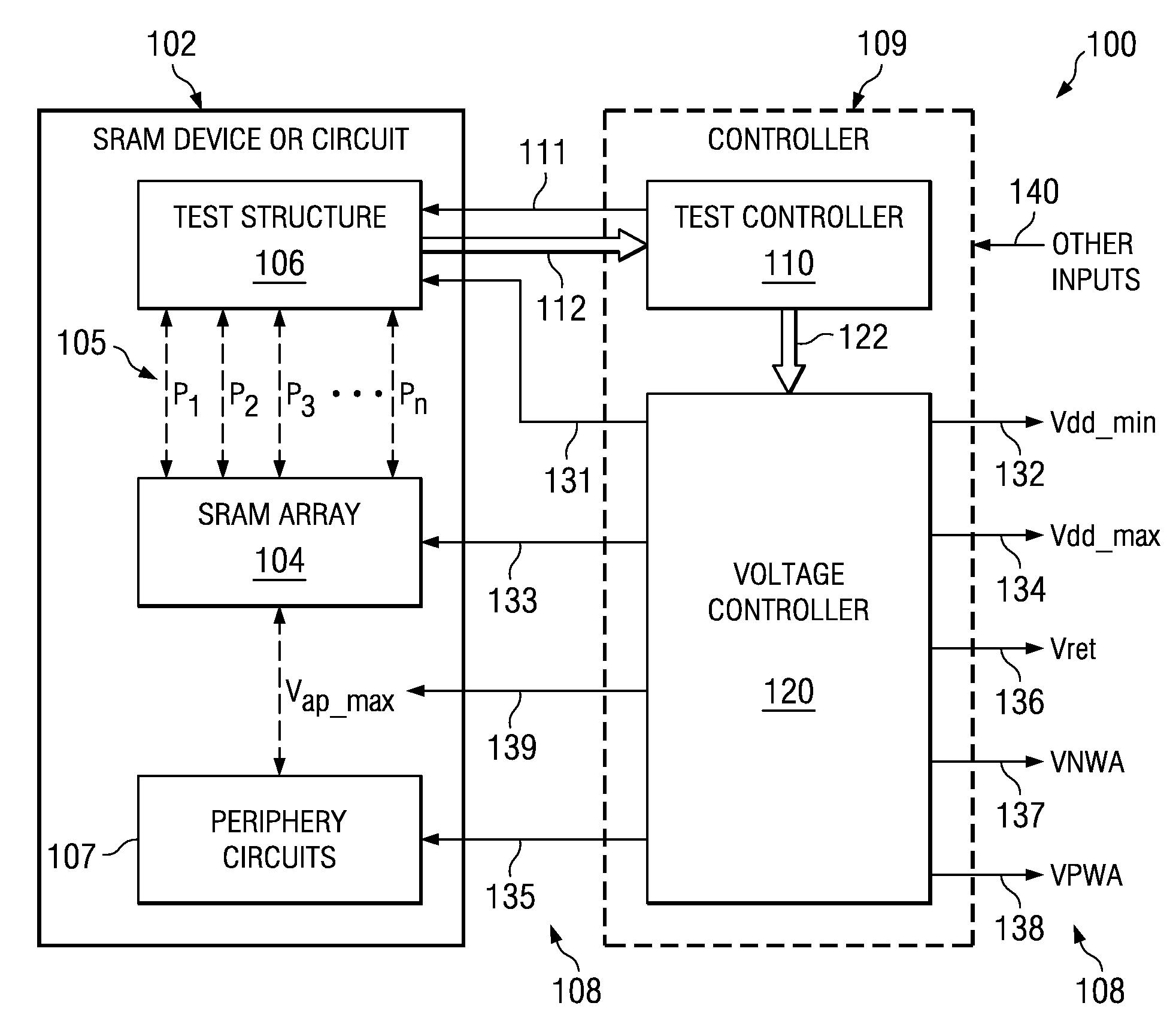
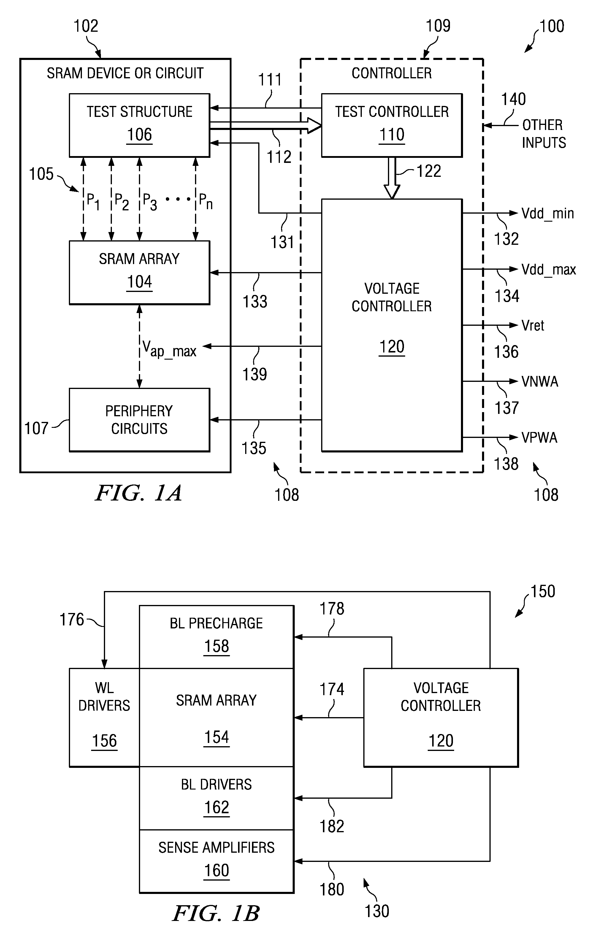
The present invention is about adaptively setting the operating voltages for SRAM based on the modeling and characterization of a test structure that evaluates or characterizes parameters that are predictive of SRAM functionality in order to reduce power while maintaining functionality and performance. The system or method includes an SRAM memory array and a test structure that provides measurable characteristics of parameters that are predictive of the functionality of the SRAM memory array and outputs data or results associated with the characteristics of the parameters. The controller or method includes analyzing the test structure data to identify an operating voltage that satisfies predetermined yield criteria and setting or generating the operating voltage for the SRAM array based on the identified operating voltage. The technical effect of the invention is to improve the efficiency and performance of SRAM memory devices by optimizing their operating voltages based on the characteristics of the transistors on a chip, which can vary from chip to chip.

Problems solved by technology

Exercising control over one or more process conditions to limit the global variation of the characteristics of the circuit elements (e.g., transistors) may in turn limit the range of operating parameters (e.g., SNM and / or Vtrip) of the SRAM cell incurred from the global variation of the circuit elements.
Thus, because of Vtrip requirements, a chip having SRAM with a low Vtp and a nominal Vtn may not be able to run at as low an operating voltage as would be allowed for the logic portion of the chip, based on frequency requirements for the logic.
Similarly, a minimum operating voltage Vmin for a chip with a low Vtn might be limited by the SNM requirements of the SRAM.
Another problem in determining an acceptable operating voltage for SRAM is that the minimum operating voltage will vary from cell to cell within an array due to random variation among the transistors.
Thus, if measurements are made on a few transistors representing the transistors in a memory array, those transistors may not be typical of the array.
Because of these factors, setting a suitable operating voltage for SRAM is challenging in view of the numerous global and local variations which affect SRAM performance.

Method used


Image

  • Adaptive voltage control for SRAM
  • Adaptive voltage control for SRAM
  • Adaptive voltage control for SRAM

Examples


Embodiment Construction

[0025]One or more aspects of the present invention are described with reference to the drawings, wherein like reference numerals are generally utilized to refer to like elements throughout, and wherein the various structures are not necessarily drawn to scale. In the following description, for purposes of explanation, numerous specific details are set forth in order to provide a thorough understanding of one or more aspects of the present invention. It may be evident, however, that one or more aspects of the present invention may be practiced with a lesser degree of these specific details. In other instances, well-known structures and devices are shown in block diagram form in order to facilitate describing one or more aspects of the present invention.

[0026]An adaptive voltage control (AVC) system is implemented to set the operating voltages of an SRAM memory device utilizing a structure or test structure that evaluates or characterizes one or more global parameters that are related...


PUM


Abstract

The present invention pertains to semiconductor memory devices, and particularly to a system and method for adaptively setting the operating voltages for SRAM for both Vtrip and SNM to reduce power while maintaining functionality and performance, based on modeling and characterizing a test structure. One embodiment comprises an SRAM array, a test structure that characterizes one or more parameters that are predictive of the SRAM functionality and outputs data of the parameters, a test controller that reads the parameters and identifies an operating voltage that satisfies predetermined yield criteria, and a voltage controller to set an operating voltage for the SRAM array based on the identified operating voltage. One method sets an operating voltage for an SRAM by reading test structure data of the parameters, analyzing the data to identify an operating voltage that satisfies predetermined yield criteria, and setting the operating voltage for the SRAM based on the identified operating voltage.

Description

FIELD OF INVENTION[0001]The present invention relates generally to integrated circuit design, and more particularly to a method and system for monitoring and adaptively setting the operating voltages for SRAM for both Vtrip and SNM, based on the modeling and characterization of a test structure to reduce power while maintaining functionality and performance.BACKGROUND OF THE INVENTION[0002]In integrated circuit (IC) manufacturing, a wafer or otherwise generally round substrate passes through a number of different fabrication stages to form one or more integrated circuits thereon. The wafer is generally formed out of a semiconductor material, such as silicon, and may pass through the different stages one or more times to form multiple layers upon the wafer. Throughout the process, the wafer and layers are treated in various manners to establish one or more semiconductor modules and elements upon the wafer. These modules can be considered the building blocks of the integrated circuits...

Claims


Application Information

Patent Timeline
Patent Type & Authority Applications(United States)
IPC IPC(8): G11C5/14
CPCG11C11/413G11C29/021G11C2029/5004G11C5/147
Inventor HOUSTON, THEODORE W.
Owner TEXAS INSTR INC
Learn More