Command Queuing Smart Storage Transfer Manager for Striping Data to Raw-NAND Flash Modules

a data stripping and data transfer technology, applied in the direction of memory address/allocation/relocation, digital storage, instruments, etc., can solve the problems of mlc flash performance, reliability and durability may decrease, and the performance of nand flash is limited

Active Publication Date: 2009-02-05
SUPER TALENT TECH CORP
View PDF23 Cites 261 Cited by
  • Summary
  • Abstract
  • Description
  • Claims
  • Application Information

AI Technical Summary

Problems solved by technology

However, NAND flash has limitations.
One limitation of NAND flash is that when storing data (writing to flash), the flash can only write from ones (1) to zeros (0).
Another limitation is that NAND flash memory has a finite number of erase cycles between 10,000 and 100,000, after which the flash wears out and becomes unreliable.
But the performance, reliability and durability may decrease for MLC flash.
A similar problem could occur with other bus protocols, such as Serial AT-Attachment (SATA), integrated device electronics (IDE), and Peripheral Components Interconnect Express (PCIe).

Method used


Image

  • Command Queuing Smart Storage Transfer Manager for Striping Data to Raw-NAND Flash Modules
  • Command Queuing Smart Storage Transfer Manager for Striping Data to Raw-NAND Flash Modules
  • Command Queuing Smart Storage Transfer Manager for Striping Data to Raw-NAND Flash Modules

Examples


Embodiment Construction

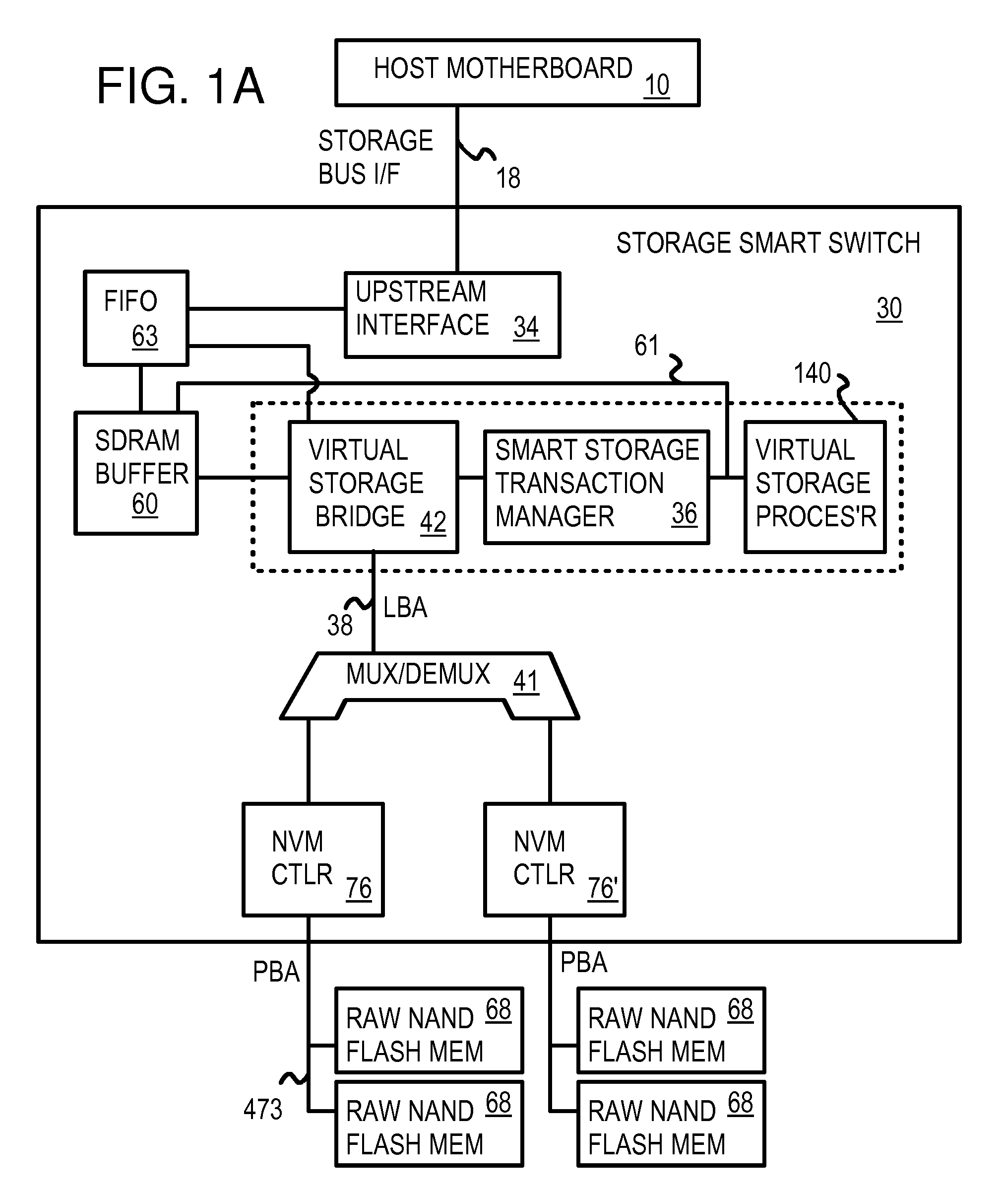
[0036]The present invention relates to an improvement in solid-state flash drives. The following description is presented to enable one of ordinary skill in the art to make and use the invention as provided in the context of a particular application and its requirements. Various modifications to the preferred embodiment will be apparent to those with skill in the art, and the general principles defined herein may be applied to other embodiments. Therefore, the present invention is not intended to be limited to the particular embodiments shown and described, but is to be accorded the widest scope consistent with the principles and novel features herein disclosed.

[0037]FIG. 1A shows a smart storage switch that connects to raw NAND flash-memory devices. Smart storage switch 30 connects to host storage bus 18 through upstream interface 34. Smart storage switch 30 also connects to raw-NAND flash memory chips 68 over a physical block address (PBA) bus 473. Transactions on logical block ad...


PUM


Abstract

A flash module has raw-NAND flash memory chips accessed over a physical-block address (PBA) bus by a NVM controller. The NVM controller is on the flash module or on a system board for a solid-state disk (SSD). The NVM controller converts logical block addresses (LBA) to physical block addresses (PBA). Data striping and interleaving among multiple channels of the flash modules is controlled at a high level by a smart storage transaction manager, while further interleaving and remapping within a channel may be performed by the NVM controllers. A SDRAM buffer is used by a smart storage switch to cache host data before writing to flash memory. A Q-R pointer table stores quotients and remainders of division of the host address. The remainder points to a location of the host data in the SDRAM. A command queue stores Q, R for host commands.

Description

RELATED APPLICATIONS[0001]This application is a continuation-in-part (CIP) of “Multi-Level Controller with Smart Storage Transfer Manager for Interleaving Multiple Single-Chip Flash Memory Devices”, U.S. Ser. No. 12 / 186,471, filed Aug. 5, 2008, which is a CIP of “High Integration of Intelligent Non-Volatile Memory Devices”, Ser. No. 12 / 054,310, filed Mar. 24, 2008, which is a CIP of “High Endurance Non-Volatile Memory Devices”, Ser. No. 12 / 035,398, filed Feb. 21, 2008, which is a CIP of “High Speed Controller for Phase Change Memory Peripheral Devices”, U.S. application Ser. No. 11 / 770,642, filed on Jun. 28, 2007, which is a CIP of “Local Bank Write Buffers for Acceleration a Phase Change Memory”, U.S. application Ser. No. 11 / 748,595, filed May 15, 2007, which is CIP of “Flash Memory System with a High Speed Flash Controller”, application Ser. No. 10 / 818,653, filed Apr. 5, 2004, now U.S. Pat. No. 7,243,185.[0002]This application is also a CIP of co-pending U.S. patent application fo...

Claims


Application Information

Patent Timeline
Patent Type & Authority Applications(United States)
IPC IPC(8): G06F12/02G11C16/02
CPCG06F12/0246G06F12/0607G11C13/0004G06F2212/7203G06F2212/7208G06F2212/1036G06F3/0607G06F3/0632
Inventor YU, FRANKLEE, CHARLES C.MA, ABRAHAM C.
Owner SUPER TALENT TECH CORP
Why Eureka
Try Eureka