Thin Multijunction Solar Cells With Plated Metal OHMIC Contact and Support

a solar cell and multi-junction technology, applied in the field of solar cell semiconductor devices, can solve the problems of presenting a number of practical difficulties relating to the appropriate choice of materials and fabrication steps, and the inability of solar cells to meet the needs of more sophisticated applications

Inactive Publication Date: 2009-02-12
EMCORE SOLAR POWER
View PDF47 Cites 84 Cited by
  • Summary
  • Abstract
  • Description
  • Claims
  • Application Information

AI Technical Summary

Benefits of technology

[0018]In another aspect, the present invention provides a solar cell that includes a semiconductor body having a sequence of layers including a first solar subcell having a first band gap; a second solar subcell disposed over the first subcell and having a second band gap smaller than the first band gap; a grading interlayer disposed ov...

Problems solved by technology

While significant progress has been made in this area, the requirement for solar cells to meet the needs of more sophisticated applications has not kept pace wi...

Method used


Image

  • Thin Multijunction Solar Cells With Plated Metal OHMIC Contact and Support
  • Thin Multijunction Solar Cells With Plated Metal OHMIC Contact and Support
  • Thin Multijunction Solar Cells With Plated Metal OHMIC Contact and Support

Examples


Embodiment Construction

[0037]Details of the present invention will now be described including exemplary aspects and embodiments thereof. Referring to the drawings and the following description, like reference numbers are used to identify like or functionally similar elements, and are intended to illustrate major features of exemplary embodiments in a highly simplified diagrammatic manner. Moreover, the drawings are not intended to depict every feature of the actual embodiment nor the relative dimensions of the depicted elements, and are not drawn to scale.

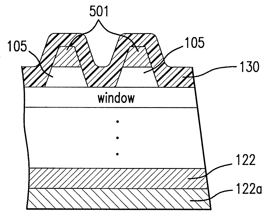
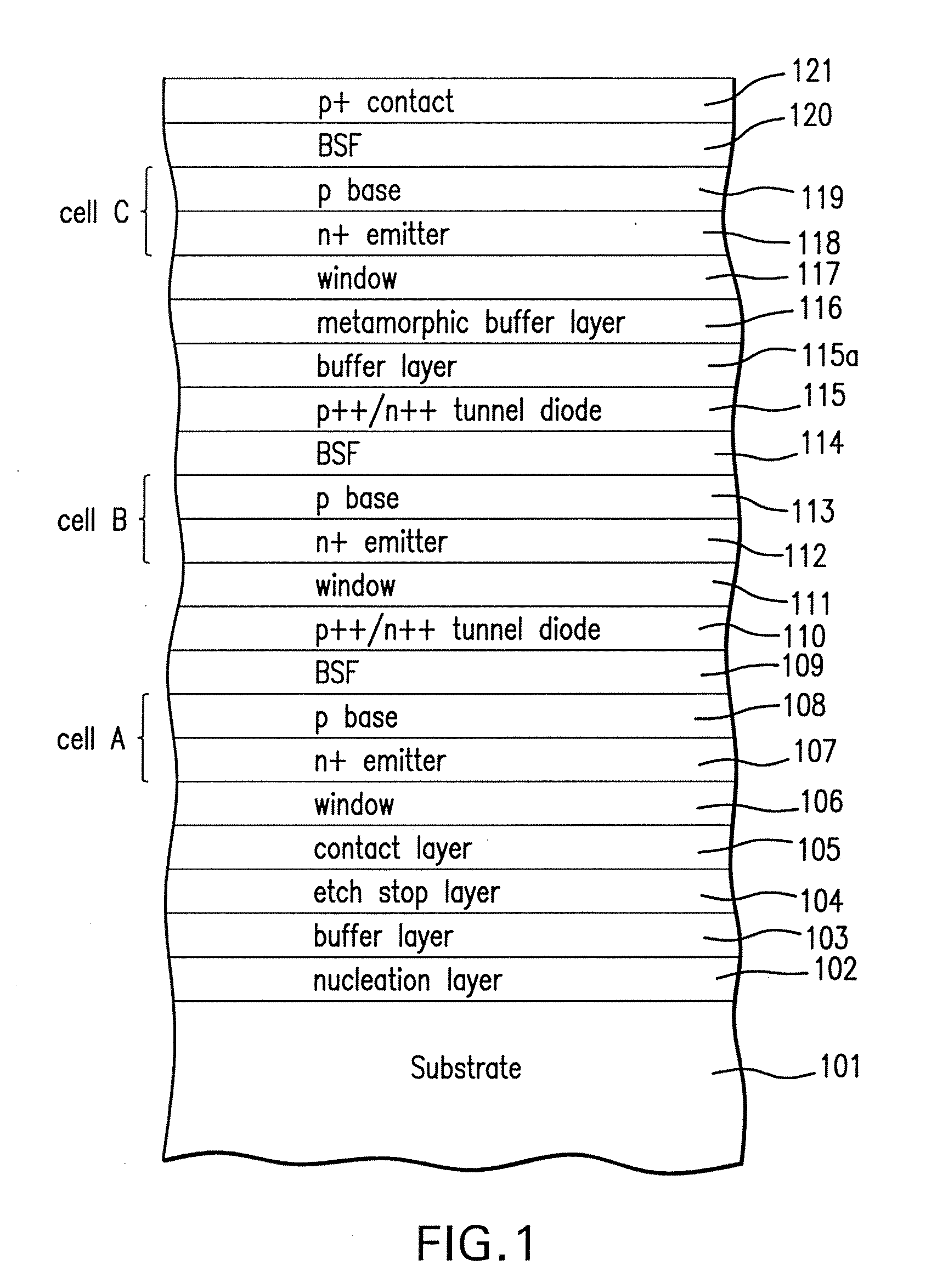
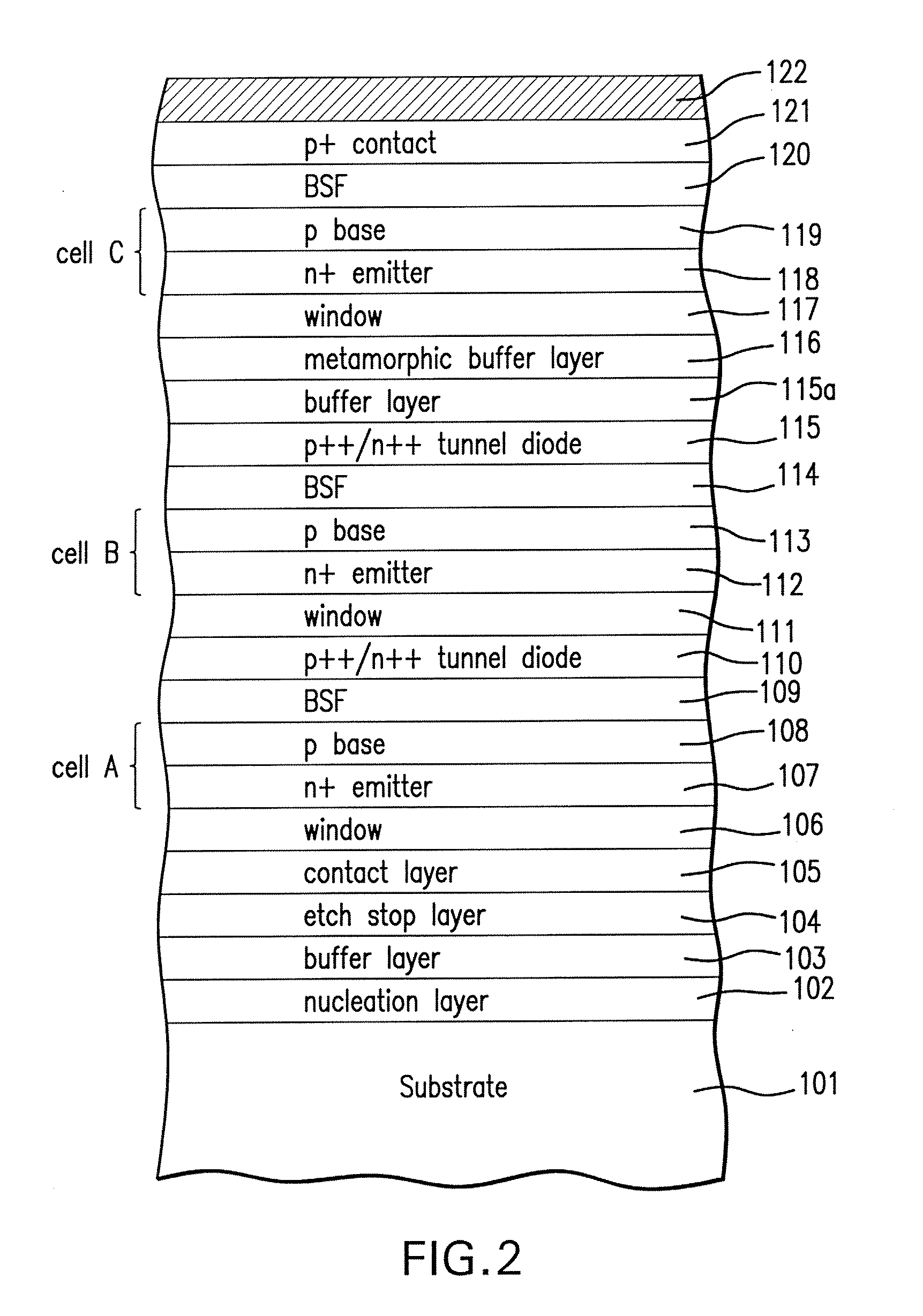
[0038]FIG. 1 depicts the multijunction solar cell according to the present invention after formation of the three subcells A, B and C on a substrate. More particularly, there is shown a substrate 101, which may be either gallium arsenide (GaAs), germanium (Ge), or other suitable material. In the case of a Ge substrate, a nucleation layer 102 is deposited on the substrate. On the substrate, or over the nucleation layer 102, a buffer layer 103, and an etch...


PUM


Abstract

A method of forming a thin multifunction solar cell in which an electroplating process is used to form a thick metal layer to give strength and support to the solar cell. The strain of the plated thick metal layer is adjusted during the process by parameter control to compensate for the strain in the other device layers, so that the curvature of the thin device can be eliminated or otherwise controlled.

Description

REFERENCE TO RELATED APPLICATIONS[0001]This application is related to co-pending U.S. patent application Ser. No. 11 / 616,596 filed Dec. 27, 2006.[0002]This application is also related to co-pending U.S. patent application Ser. No. 11 / 445,793 filed Jun. 2, 2006.GOVERNMENT RIGHTS STATEMENT[0003]This invention was made with government support under Contract No. FA9453-04-2-0041 awarded by the U.S. Air Force. The Government has certain rights in the invention.BACKGROUND OF THE INVENTION[0004]1. Field of the Invention[0005]The present invention relates to the field of solar cell semiconductor devices, and particularly to integrated semiconductor structures including a multijunction solar cell including an electroplated ohmic contact.[0006]2. Description of the Related Art[0007]Photovoltaic cells, also called solar cells, are one of the most important new energy sources that have become available in the past several years. Considerable effort has gone into solar cell development. As a res...

Claims


Application Information

Patent Timeline
IPC IPC(8): H01L31/042H01L21/62
CPCH01L31/022433H01L31/068H01L31/06875Y02E10/547H01L31/1844Y02E10/544H01L31/1804Y02P70/50
Inventor VARGHESE, TANSENCORNFELD, ARTHURXIE, MICHELLE
Owner EMCORE SOLAR POWER
Why Eureka
Try Eureka