

Light emitting diodes with current spreading layer
a technology of light-emitting diodes and current spreading layers, which is applied in the direction of basic electric elements, electrical equipment, semiconductor devices, etc., can solve the problems of increasing manufacturing costs, not being suitable for growing algainp crystal layers, and not being suitable for thick window layers for some device configurations
- Summary
- Abstract
- Description
- Claims
- Application Information
AI Technical Summary
Benefits of technology
Problems solved by technology
Method used
Image

Examples
first embodiment
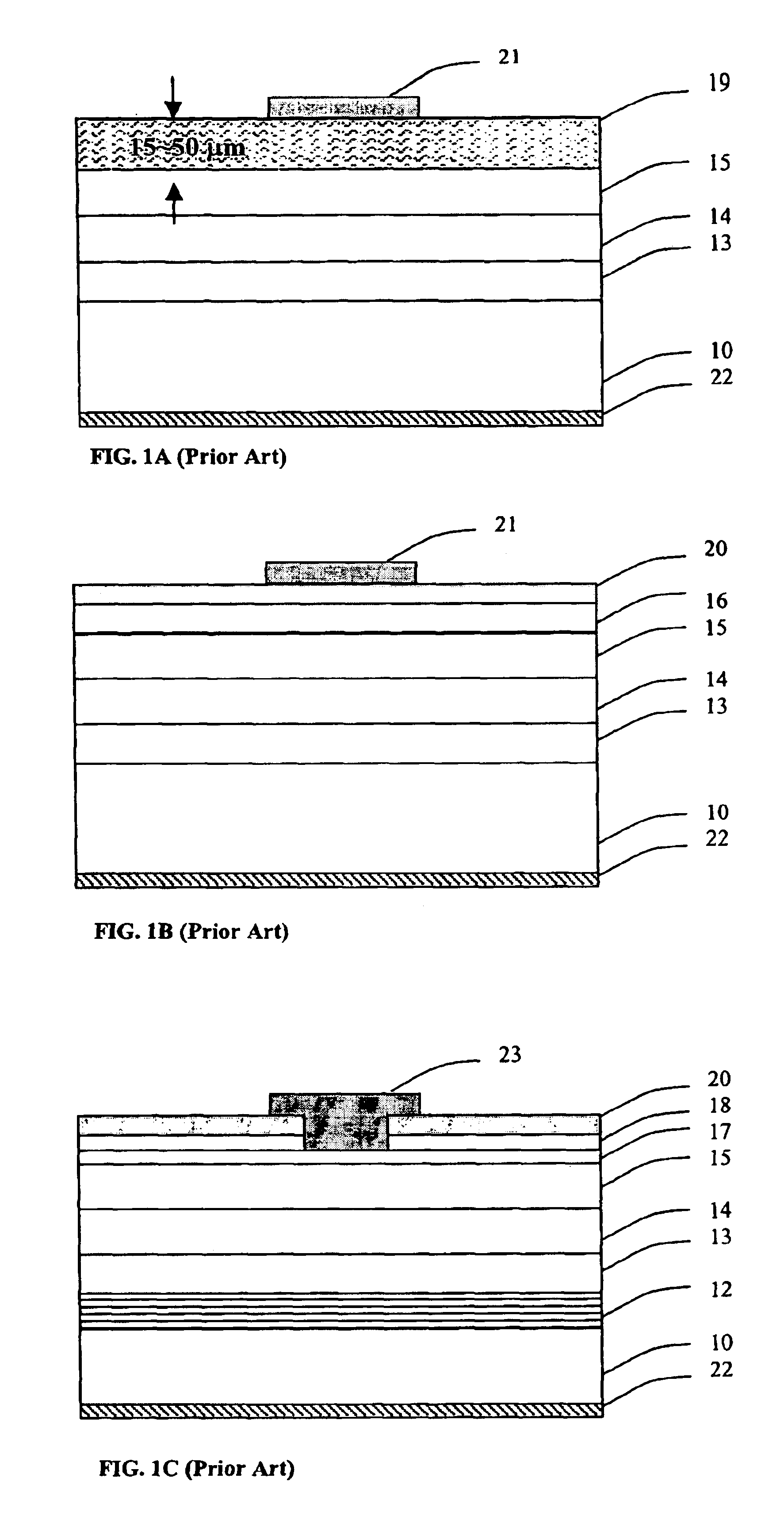
[0027]In the present invention, a light emitting diode comprises an ultra-thin composite metallic layer between the transparent current spreading layer and p-type semiconductor layer to form a good ohmic contact without sacrificing the light transparency. The ultra-thin metallic layer comprises at least one type of metal. Typically two metal layers such as a first layer of titanium and a second layer of gold may be deposited to form the ultra-thin composite layer. Here, the titanium layer serves as surface cleaning and adhesive agent when deposited over or on the p-type semiconductor layer. The second transparent current spreading layer is a thick ITO layer or its equivalents. The ultra-thin composite metallic layer will facilitate connection to the ITO layer to form an excellent ohmic contact after Rapid Thermal Annealing (RTA) treatment around 330˜440° C. for 0.5 to 2 minutes, which causes some of the metallic layer to diffuse into the ITO layer. The metal thickness of the ultra-t...
second embodiment
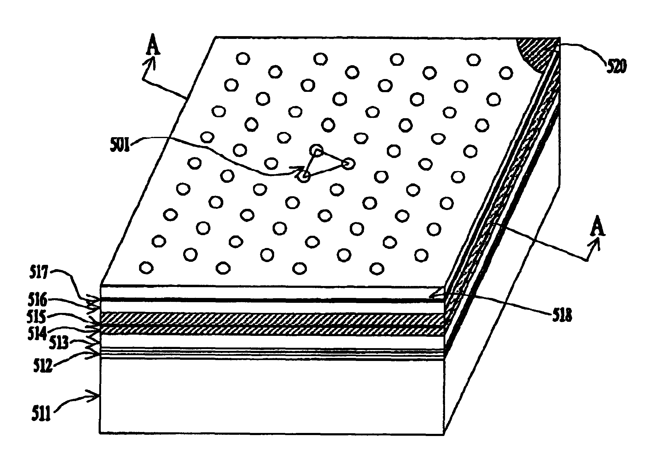
[0033]A second embodiment in the present invention is illustrated schematically in FIG. 7-9 for the LED structure and LED device of GaN-based materials. FIG. 7 shows the top metal (Ni / Au etc.) bonding pad 321 of the LED.
[0034]As illustrated by the structures shown in FIG. 8 and FIG. 9, the LED structure is first grown on the lattice-mismatched insulating sapphire substrate 310 using MOCVD. A very thin low temperature GaN nucleation layer 311 is grown, followed by a thick n-type GaN 312. The active layer 313 comprises several InGaN / GaN strained MQWs. Finally, the p-AlGaN upper cladding layer 314 for electrical confinement and p-GaN contact layer 315 are deposited.
[0035]In the conventional LED structure, the current spreading layer is a thin semi-transparent metal layer such as NiO / Au (transmission is around 60% with thickness of 10 / 30 nm). In the present invention, an ultra-thin composite metallic layer such as Ti / Au, Ti / Au—Zn, Ti / Au—Be, Ti / In—Be or Ni / Au 316, followed by a transpare...
PUM
 Abstract
Description
Claims
Application Information