Technique For Preparing Precursor Films And Compound Layers For Thin Film Solar Cell Fabrication And Apparatus Corresponding Thereto

a technology of precursor films and compound layers, which is applied in the direction of sustainable manufacturing/processing, thermoelectric devices, and final product manufacturing, etc., can solve the problems of poor adhesion characteristics, low band gap, and high cost of equipment, and achieve low throughput, low material utilization, and high equipment cost

Inactive Publication Date: 2007-04-26
SOLOPOWER
View PDF32 Cites 112 Cited by
  • Summary
  • Abstract
  • Description
  • Claims
  • Application Information

AI Technical Summary

Problems solved by technology

However, the cost of electricity generated using silicon-based solar cells is higher than the cost of electricity generated by the more traditional methods.
Absorbers containing no Ga, on the other hand, have a low bandgap of about 1 eV and also have poor adhesion characteristics to their substrate, limiting their efficiencies.
However, low materials utilization, high cost of equipment, difficulties faced in large area deposition and relatively low throughput are some of the challenges faced in commercialization of the co-evaporation approach.
Such techniques may yield good quality absorber layers and efficient solar cells, however, they suffer from the high cost of capital equipment, and relatively slow rate of production.
Also physical vapor deposition (PVD) techniques such as sputtering and evaporation, although flexible in changing the deposition sequence of the elements forming a metallic stack, have certain drawbacks in terms of ability to form stacks with layers of un-alloyed, pure materials as will be discussed later.
Although low-cost in nature, both of these techniques were found to yield CIS films with poor adhesion to the Mo contact layer.
One problem area was identified as peeling of the compound films during solar cell processing.
It was stated, in the absence of Pd or Pt interfacial layers, the KCN etching step led to film peeling problems if the Cu to Group IIIA ratio was larger than 1.6.
Wet processing techniques such as electrodeposition and electroless deposition, although lower cost than the PVD approaches such as evaporation and sputtering, have their unique challenges.
In an electrodeposition process, however, there have been limitations in forming metallic stacks comprising various different metals.
For Ga deposition, which is challenging due to hydrogen evolution, even larger negative voltages are required.
However, after selenization such stacks yielded compound layers with poor morphology and poor adhesion to the base or the Mo coated substrate as was discussed before.
This approach would not be low cost because preparation of Cu—Ga alloy sputtering targets is in itself expensive and utilization of the target material is very low (typically lower than 40%) in a sputtering approach.

Method used


Image

  • Technique For Preparing Precursor Films And Compound Layers For Thin Film Solar Cell Fabrication And Apparatus Corresponding Thereto
  • Technique For Preparing Precursor Films And Compound Layers For Thin Film Solar Cell Fabrication And Apparatus Corresponding Thereto
  • Technique For Preparing Precursor Films And Compound Layers For Thin Film Solar Cell Fabrication And Apparatus Corresponding Thereto

Examples


example 1

Cu / Ga / Cu / In Stack Formation:

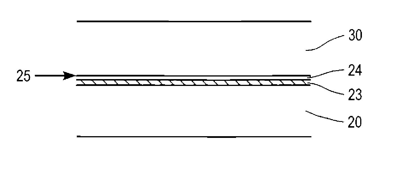
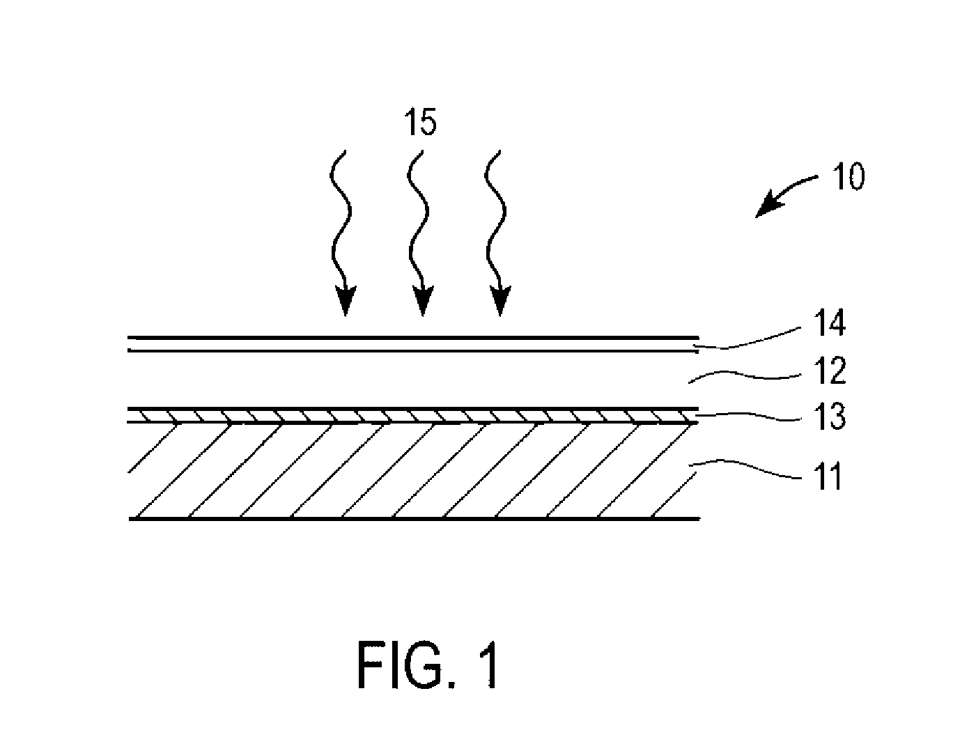
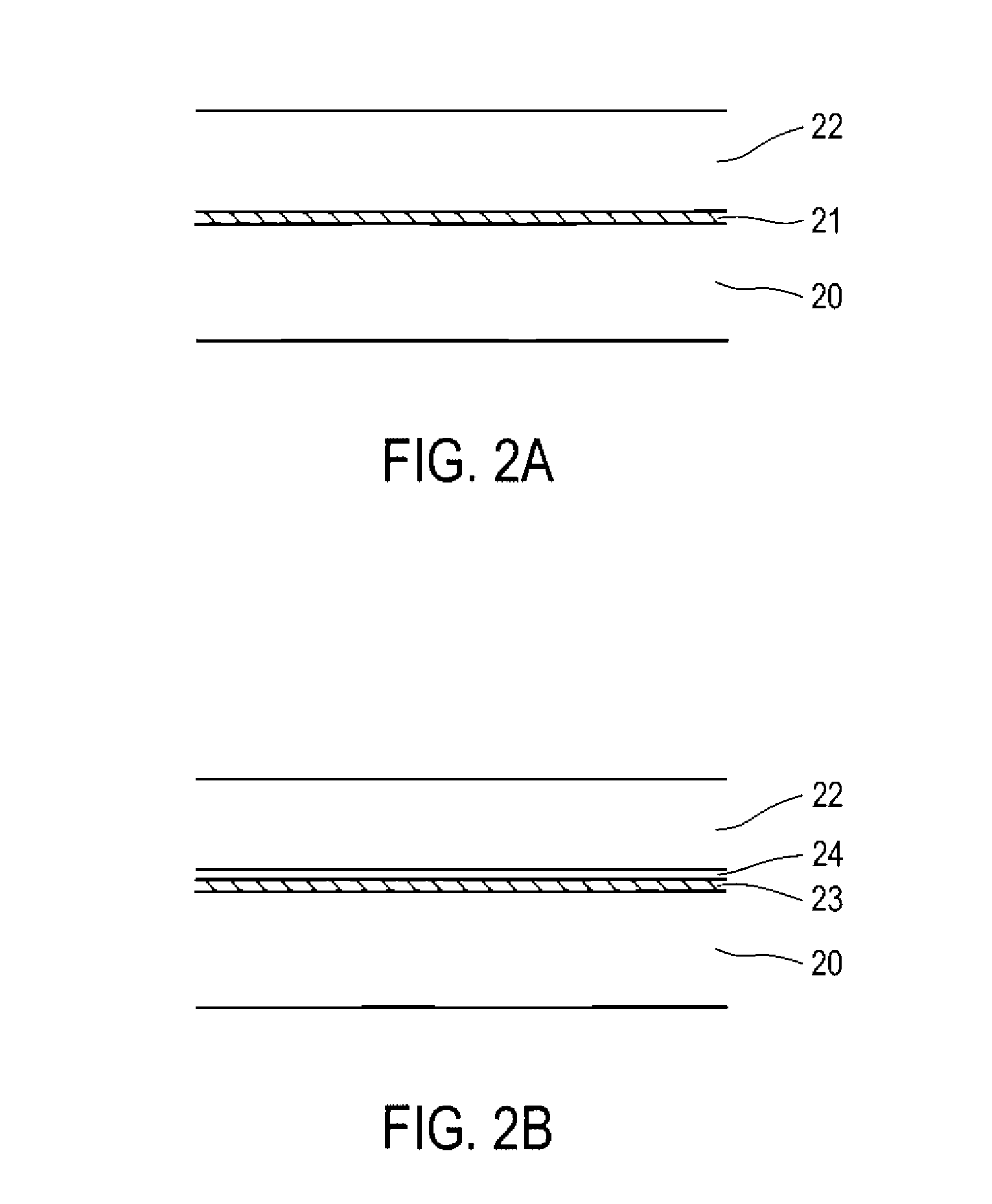
[0032] A glass / Mo base is used in the experiment. Mo is sputter deposited to a thickness of about 700 nm on the glass sheet. Then SOLCu is employed to electroplate 150 nm thick Cu sub-layer over the Mo surface at a current density of 5 mA / cm2. The resulting Cu sub-layer is uniform and smooth with 3-5 nm surface roughness. A 100 nm thick Ga layer is deposited on the Cu sub-layer using SOLGa at a current density of 10 mA / cm2. A smooth and shiny silver-colored layer is obtained. SOLCu solution is utilized again to deposit 50 nm thick Cu sub-layer over the Ga layer at a current density of 5 mA / cm2. No Ga is lost into the SOLCu during Cu plating since the plating potential of Cu with respect to a calomel electrode placed into the solution was measured to be in the (−1 to −2 V) range. Such high cathodic potential protects the Ga layer from dissolving and also allows deposition of a small-grained and continuous Cu sub-layer on the Ga surface. After the formati...

example 2

Cu / Ga / Cu / In / Cu Stack Formation:

[0033] A glass / Mo base is used. Mo is sputter deposited to a thickness of about 700 nm on the glass sheet. Then SOLCu is employed to electroplate 150 nm thick Cu sub-layer over the Mo surface at a current density of 5 mA / cm2. The resulting Cu sub-layer is uniform and smooth with 3-5 nm surface roughness. A 100 nm thick Ga layer is deposited on the Cu sub-layer using SOLGa at a current density of 10 mA / cm2. A smooth and shiny silver-colored layer is obtained. SOLCu solution is utilized again to deposit 10 nm thick Cu sub-layer over the Ga layer at a current density of 5 mA / cm2. After the formation of the 10 nm thick Cu sub-layer over the 100 nm thick Ga layer, SOLIn is used at 15 mA / cm2 current density to form a 400 nm thick In layer. Over the In layer, another Cu sub-layer is plated using SolCu to a thickness of 40 nm. No In is lost into the SOLCu during Cu plating since the plating potential of Cu with respect to a calomel electrode placed into the ...

example 3

Cu / In / Cu / Ga Stack Formation:

[0034] A glass / Mo base is used. Mo is sputter deposited to a thickness of about 700 nm on the glass sheet. Then SOLCu is employed to electroplate 150 nm thick Cu sub-layer over the Mo surface at a current density of 5 mA / cm2. The resulting Cu sub-layer is uniform and smooth with 3-5 nm surface roughness. A 400 nm thick In layer is deposited on the Cu sub-layer using SOLIn at a current density of 15 mA / cm2. SOLCu solution is utilized again to deposit 50 nm thick Cu sub-layer over the In layer at a current density of 5 mA / cm2. No In is lost into the SOLCu during Cu plating since the plating potential of Cu with respect to a calomel electrode placed into the solution is measured to be in the (−1 to −2 V) range. Such high cathodic potential protects the In layer from dissolving and also allows deposition of a small-grained and continuous Cu layer on the In surface, After the formation of the 50 nm thick Cu sub-layer over the 400 nm thick Ga layer, SOLGa is ...


PUM

PropertyMeasurementUnit
molar ratioaaaaaaaaaa

Abstract

The present invention advantageously provides for, in different embodiments, improved contact layers or nucleation layers over which precursors and Group IBIIIAVIA compound thin films adhere well and form high quality layers with excellent micro-scale compositional uniformity. It also provides methods to form precursor stack layers, by wet deposition techniques such as electroplating, with large degree of freedom in terms of deposition sequence of different layers forming the stack.

Description

Claim of Priority [0001] This application claims priority to U.S. Provisional Appln. Ser. No. 60 / 781,984 filed Mar. 13, 2006, entitled “Technique for Preparing Precursor Layers For Thin Film Solar Cell Fabrication”, to U.S. Provisional Appln. Ser. No. 60 / 807,703 filed Jul. 18, 2006 entitled “Technique for Preparing Precursor Layers For Thin Film Solar Cell Fabrication”, to U.S. Provisional Appln. Ser. No. 60 / 729,846 filed Oct. 24, 2005 entitled “Method and Apparatus for Thin Film Solar Cell Manufacture”, and to U.S. Provisional Appln. Ser. No. 60 / 756,750 filed Jan. 6, 2006 entitled “Precursor Copper Indium, and Gallium for Selenide (Sulfide) Compound Formation”, all of which are expressly incorporated herein in their entirety. This application is also a continuation-in-part of U.S. application Ser. No. 11 / 266,013 filed Nov. 2, 2005 entitled “Technique and Apparatus for Depositing Layers of Semiconductors for Solar Cell and Module Fabrication”, the contents of which are expressly inc...

Claims


Application Information

Patent Timeline
Patent Type & Authority Applications(United States)
IPC IPC(8): H01L21/84H01L29/08H01L35/24H01L21/00H01L51/00
CPCH01L21/02425H01L21/02491H01L21/02568H01L21/02614H01L21/02628H01L21/02658H01L31/022425H01L31/022466H01L31/0296H01L31/0322H01L31/0392H01L31/0749H01L31/1844Y02E10/541Y02E10/544H01L21/0237H01L31/022483H01L31/03925H01L31/03928Y02P70/50H01L21/06H01L29/04H01L29/06H01L31/0445
Inventor BASOL, BULENT M.
Owner SOLOPOWER
Why Eureka
Try Eureka