Fingerprint sensor and fabrication method thereof

a fingerprint sensor and fabrication method technology, applied in the field of fingerprint sensors, can solve the problems of insufficient security management of personal information, high cost, and inability to easily apply to portable terminals, and achieve the effect of increasing the speed of fingerprint authentication

Inactive Publication Date: 2008-07-15
SAMSUNG ELECTRONICS CO LTD
View PDF7 Cites 115 Cited by
  • Summary
  • Abstract
  • Description
  • Claims
  • Application Information

AI Technical Summary

Benefits of technology

[0010]The present invention provides a fingerprint sensor of an ultrasonic type in which components can be fabricated together using a micro-electric mechanical system (MEMS) process to have a thin film shape so as to increase a fingerprint authentication speed, and a fabrication method thereof.

Problems solved by technology

This gives rise to a social problem of security management of personal information.
Thus, a process of inputting identifications (IDs) and passwords is not sufficient to secure personal information.
Thus, the ultrasonic type fingerprint sensor adopts a separately fabricated probe 102, which scans a fingerprint, and thus is costly and not easily applied to portable terminals.
Also, the ultrasonic type fingerprint sensor obtains an image of a fingerprint using a scan method, resulting in slow fingerprint authentication.

Method used


Image

  • Fingerprint sensor and fabrication method thereof
  • Fingerprint sensor and fabrication method thereof
  • Fingerprint sensor and fabrication method thereof

Examples


Embodiment Construction

[0029]Hereinafter, a fingerprint sensor according to an embodiment of the present invention will be described in detail with reference to the attached drawing.

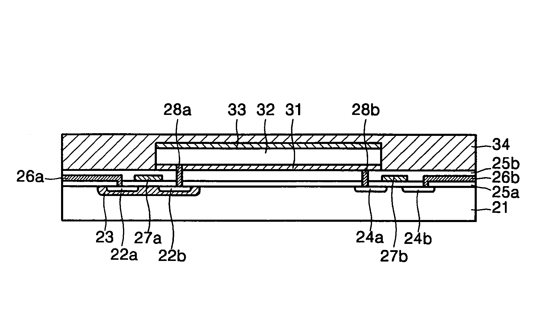
[0030]FIG. 2 is a cross-sectional view of a fingerprint sensor according to an embodiment of the present invention. A CMOS structure in which a negative-channel metal-oxide semiconductor (NMOS) structure and a positive-channel metal-oxide semiconductor (PMOS) structure are formed on an n-type or p-type substrate is formed as a lower structure of the fingerprint sensor according to the present invention. This will be briefly explained as follows. Here, a case where an n-type substrate is used will be explained. A portion of the surface of an n-type substrate 21 is doped with a p-type dopant to form a p-type doped layer 23. An n-type source 22a and an n-type drain 22b are formed in the portion of the surface of the n-type substrate 21 in which the p-type doped layer 23 has been formed. A p-type source 24a and a p-type drain 24b ...


PUM


Abstract

Provided are a fingerprint sensor and a fabrication method thereof. The fingerprint sensor includes: a complementary metal-oxide semiconductor structure which is formed on a substrate that is doped with a first type dopant; an insulating layer which is formed on the complementary metal-oxide semiconductor structure; a lower electrode which is formed in a central portion of the insulating layer; a piezoelectric region which is formed on the lower electrode; an upper electrode which is formed on the piezoelectric layer; and a fingerprint contact layer which is formed to cover a portion of an upper surface of the insulating layer on which the lower electrode has not been formed, the lower electrode, the piezoelectric region, and the upper electrode.

Description

BACKGROUND OF THE INVENTION[0001]This application claims the priority of Korean Patent Application No. 2003-81724, filed on Nov. 18, 2003, in the Korean Intellectual Property Office, the disclosure of which is incorporated herein in its entirety by reference.[0002]1. Field of the Invention[0003]The present invention relates to a fingerprint sensor and a fabrication method thereof, and more particularly, to a fingerprint sensor adopting a complementary metal-oxide semiconductor (CMOS) structure on which a piezoelectric region for generating ultrasonic waves is formed, so as to be fabricated using a simple process and to authenticate a fingerprint at a high speed.[0004]2. Description of the Related Art[0005]In the past, goods were purchased through off-line direct trades by cash payments. However, economic and social advances have changed this way of trade into today's transactions by credit cards, off-line e-money, or the like. This gives rise to a social problem of security manageme...

Claims


Application Information

Patent Timeline
Patent Type & Authority Patents(United States)
IPC IPC(8): G06K9/00A61B5/117B06B1/06G06T1/00H01L21/00H01L21/8238H01L27/092H01L41/08H01L41/18H01L41/187H01L41/193H01L41/22H01L41/311
CPCG06K9/0002G06V40/1306G06F18/00
Inventor NAM, YUN-WOO
Owner SAMSUNG ELECTRONICS CO LTD
Why Eureka
Try Eureka