Display Device

a technology of a display device and a pixel area, which is applied in the direction of identification means, instruments, drug compositions, etc., can solve the problems of arranging all the component elements in one pixel area, and achieve the effect of efficient arranging the component elements of a pixel circuit in a given pixel area

Active Publication Date: 2009-02-12
SAMSUNG DISPLAY CO LTD
View PDF38 Cites 6 Cited by
  • Summary
  • Abstract
  • Description
  • Claims
  • Application Information

AI Technical Summary

Benefits of technology

[0017]It is an aspect of the present invention to provide a light-emitting display panel and a light-emitting display capable of efficiently arranging component elements of a pixel circuit in a given pixel area.

Problems solved by technology

Therefore, such a construction requires a large number of elements such as transistors and capacitors formed in one pixel and hence a large number of interconnections to transfer voltages or signals, so there is a considerable difficulty in arranging all the component elements in one pixel area.

Method used


Image

  • Display Device
  • Display Device
  • Display Device

Examples


Embodiment Construction

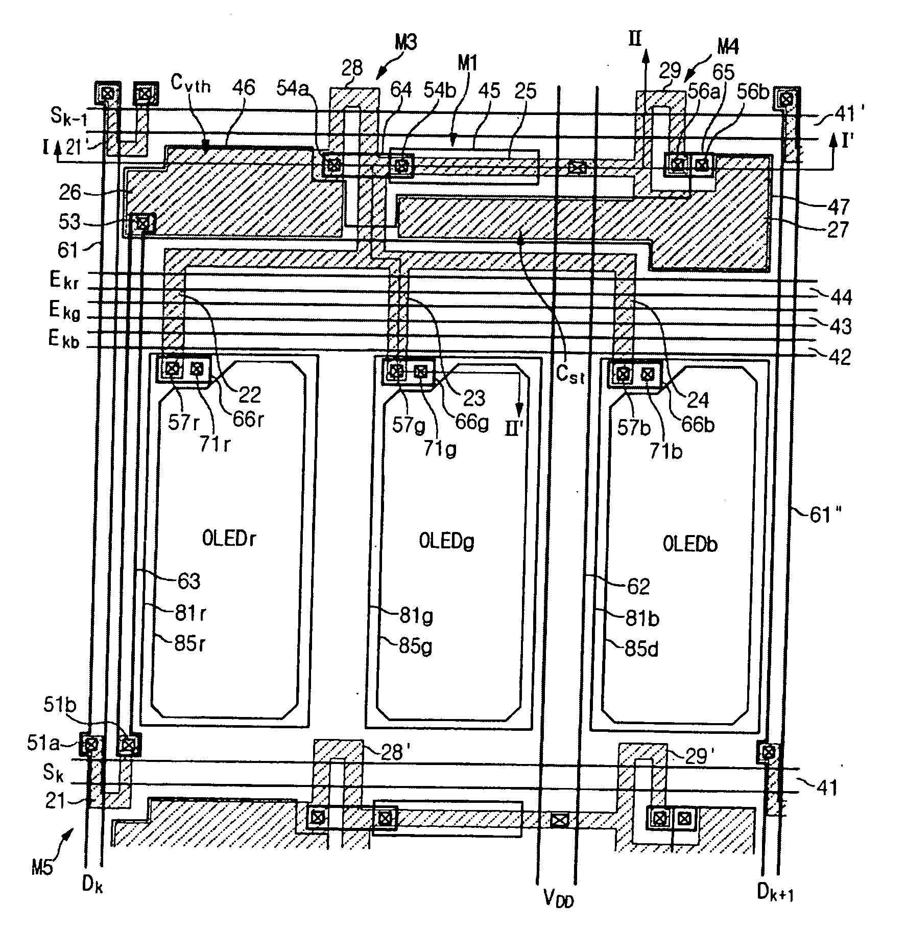
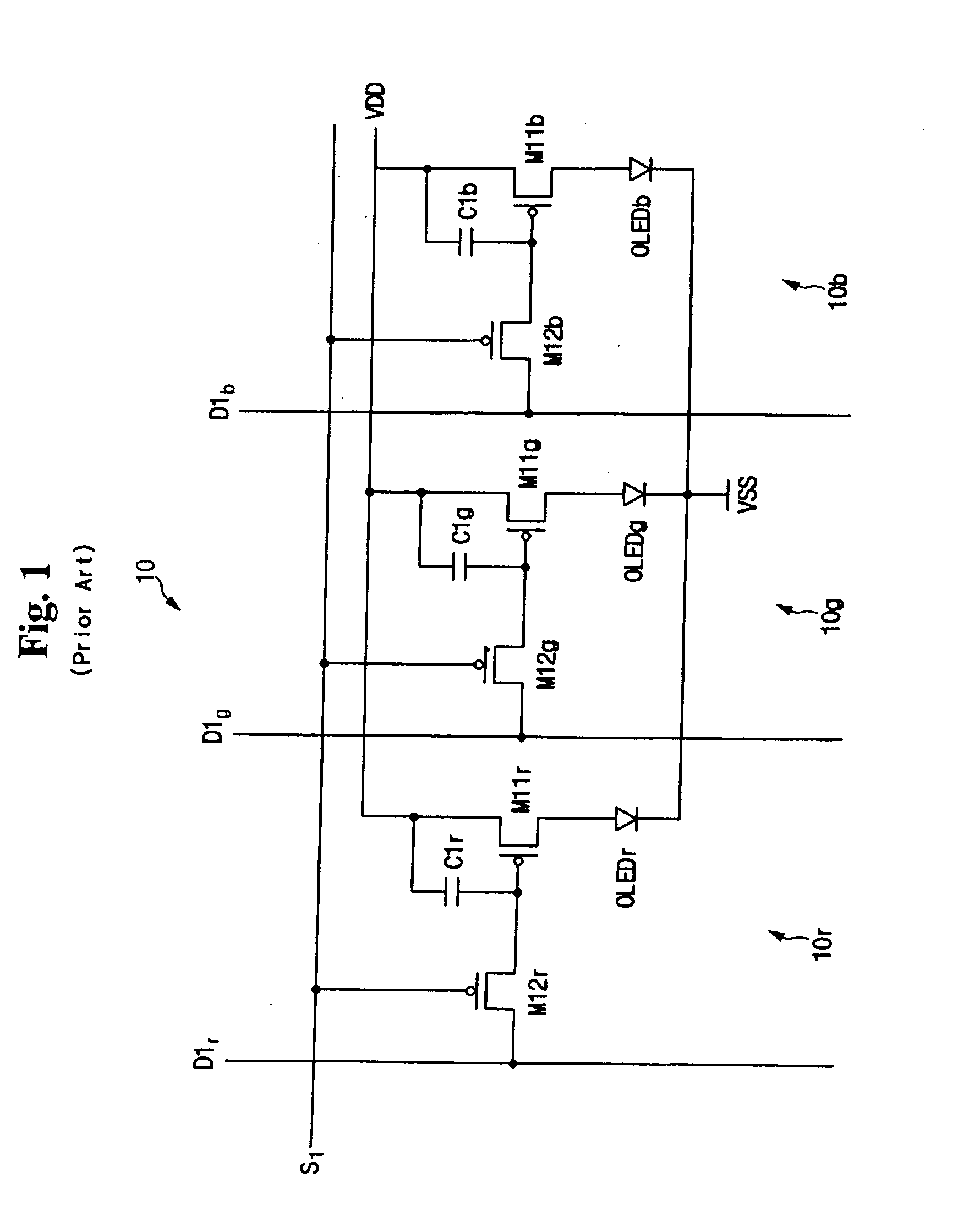
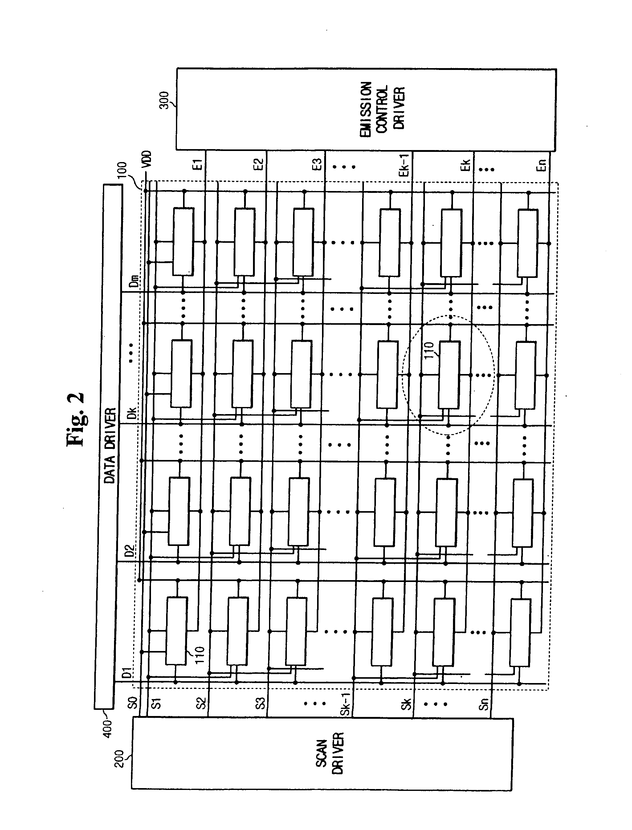
[0038]In the following detailed description, exemplary embodiment(s) of the present invention are shown and described, by way of illustration. As those skilled in the art would recognize, the described exemplary embodiment(s) may be modified in various ways, all without departing from the spirit or scope of the present invention. Accordingly, the drawings and description are to be regarded as illustrative in nature, and not restrictive.

[0039]There may be parts shown in the drawings, or parts not shown in the drawings, that are not discussed in the specification as they are not essential to a complete understanding of the invention. Like reference numerals designate like elements. When it is stated that a first component is coupled to a second component, the first and second components may be coupled directly to each other or a third component may be positioned between the first component and the second component. Also, a part such as a layer, a film, an area, or a plate is on anothe...


PUM


Abstract

A current pixel circuit of a display device includes a switching transistor which may be turned on in response to the current selection signal to transfer a data signal, a driving transistor for outputting a current corresponding to the data signal, and first and second transistors being turned on in response to the previous selection signal. In the display device, the gate electrodes of the switching transistor of a previous pixel and the first and second transistors of the current pixel are coupled to one scan line for transferring the previous selection signal. Accordingly, the transistors are arranged in the order of the switching transistor of the previous pixel and the first and second transistors of the current pixel on the scan line at an area between two adjacent data lines.

Description

CROSS REFERENCE TO RELATED APPLICATION[0001]This application is a divisional of U.S. application Ser. No. 11 / 129,016, filed on May 13, 2005 which claims priority to and the benefit of Korean Patent Application No. 10-2004-0036855 filed on May 24, 2004 in the Korean Intellectual Property Office, the entire content of which is incorporated herein by reference.BACKGROUND OF THE INVENTION[0002](a) Field of the Invention[0003]The present invention relates to a displaying device. More specifically, the present invention relates to an organic electro-luminescence (herein also referred to as EL) light-emitting display using the electro-luminescence of an organic material.[0004](b) Description of the Related Art[0005]The organic EL light-emitting display, which is a device for electrically exciting an organic fluorescent material to emit a light, drives n×m organic light-emitting elements arranged in a matrix to represent an image.[0006]The organic light-emitting element, also called “organi...

Claims


Application Information

Patent Timeline
Patent Type & Authority Applications(United States)
IPC IPC(8): H01L29/04H01L51/50B41J2/45G09F9/30G09G3/20G09G3/30G09G3/32H01L27/32H05B33/14H05B44/00
CPCG09G3/3233G09G2300/0452G09G2300/0465G09G2300/0804G09G2300/0819H01L27/3244G09G2300/0861G09G2310/0235G09G2310/0251G09G2320/043H01L27/3211G09G2300/0852A61P1/16A61P11/00A61P13/12A61P9/10A61P9/12H10K59/35H10K59/131H01L27/124H10K59/1213H10K59/12
Inventor KWAK, WON-KYU
Owner SAMSUNG DISPLAY CO LTD
Why Eureka
Try Eureka