Dll circuit, semiconductor memory device using the same, and data processing system

a technology of semiconductor memory and circuit, applied in the direction of digital storage, pulse automatic control, instruments, etc., can solve the problems of inability to obtain the number of adjustment steps necessary to determine the delay amount, and the inability to adjust the adjustment precision of the theoretical value. , to achieve the effect of increasing the adjustment precision of the second delay line, wasting tim

Inactive Publication Date: 2009-02-12
LONGITUDE SEMICON S A R L
View PDF5 Cites 11 Cited by
  • Summary
  • Abstract
  • Description
  • Claims
  • Application Information

AI Technical Summary

Benefits of technology

[0008]Another object of the present invention is to provide a DLL circuit that can determine a delay amount at a fast speed even when the number of bits of a count signal for adjusting an FDL is increased, and a semiconductor memory device using the DLL circuit.
[0009]Still another object of the present invention is to provide a DLL circuit of which adjustment precision of the FDL is increased, and a semiconductor memory device using the DLL circuit.
[0025]According to one aspect of the present invention, the DLL circuit controls the second delay line based on the binary search method. Therefore, even if the number of bits of the count signal to adjust the second delay line is increased, a delay amount can be determined at a high speed. On the other hand, when the frequency of the clock signal is very high, the adjustment pitch of the first delay line to the clock cycle is too coarse, and therefore, the adjustment using the first delay line is not substantially effective. Consequently, when the first delay line is controlled using the binary search method, it takes a wasteful time. However, according to the present invention, because the first delay line is controlled by the linear search method, the control of the first delay line can be completed immediately.
[0026]Further according to another aspect of the present invention, the DLL circuit has the first MOS transistor inserted into between the second MOS transistor to which a predetermined value of the count value is supplied and the power source line. Further, the intermediate potential is supplied to the gate of this transistor. Therefore, the first MOS transistor becomes in the conducted state in the saturation region. Consequently, the current supplied to the source of the second MOS transistor becomes at a constant value, and the adjustment precision of the second delay line can be increased.

Problems solved by technology

However, when the adjustment pitch of the FDL is set small, the number of adjustment steps necessary to determine the delay amount is necessary by that amount.
As a result, it takes time for the adjustment.
However, actually, adjustment precision of the theoretical value cannot be often obtained.

Method used


Image

  • Dll circuit, semiconductor memory device using the same, and data processing system
  • Dll circuit, semiconductor memory device using the same, and data processing system
  • Dll circuit, semiconductor memory device using the same, and data processing system

Examples


Embodiment Construction

[0040]Preferred embodiments of the present invention will now be explained in detail with reference to the drawings.

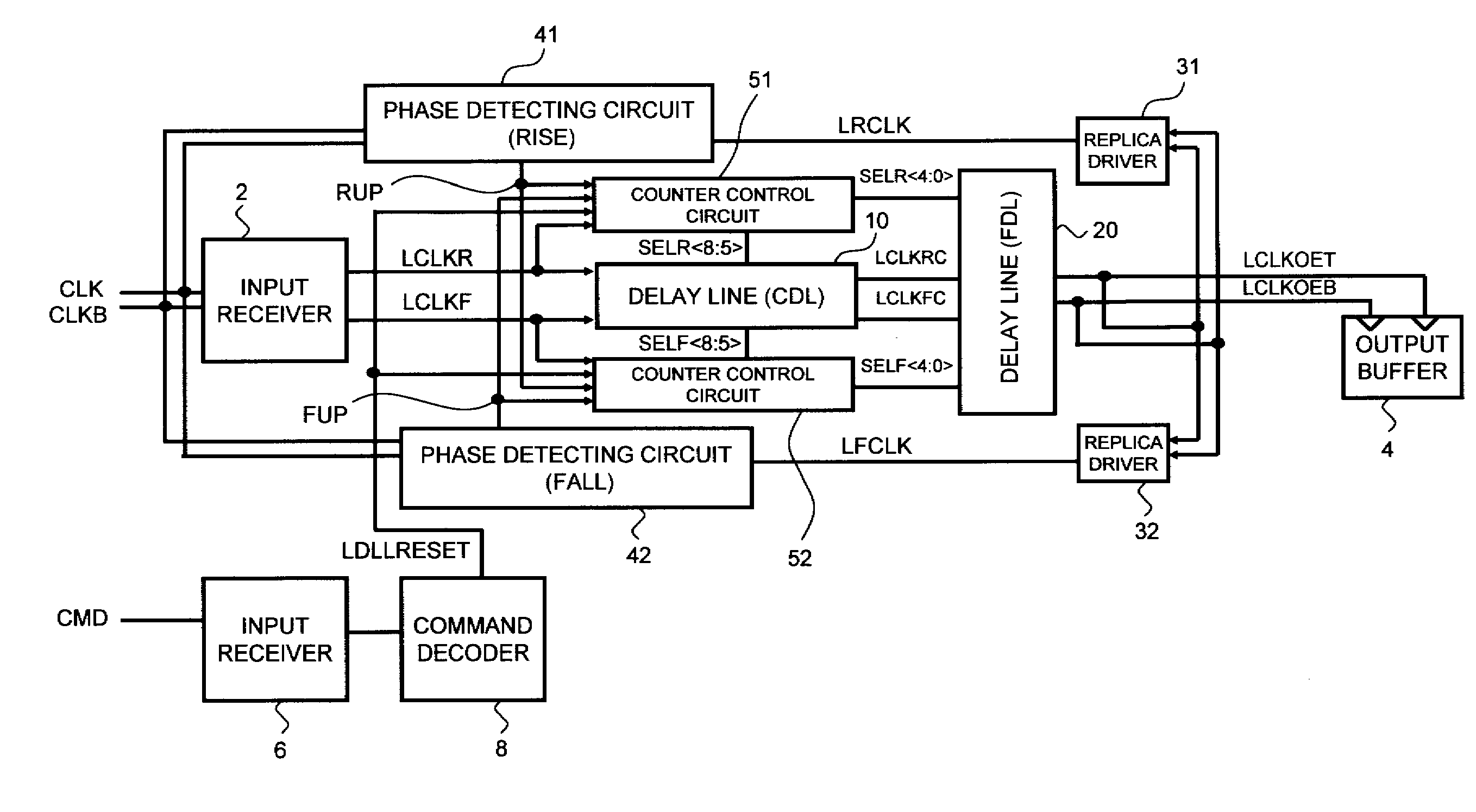
[0041]FIG. 1 is a block diagram showing a configuration of a DLL circuit according to a preferred embodiment of the present invention.

[0042]As shown in FIG. 1, the DLL circuit according to the present embodiment includes an input receiver 2 that generates complementary clock signals LCLKR and LCLKF by receiving complementary clock signals CLK and CLKB, a first delay line 10 (CDL) that generates clock signals LCLKRC and LCLKFC by delaying the clock signals LCLKR and LCLKF at a relatively coarse adjustment pitch, and a second delay line 20 (FDL) that generates clock signals LCLKOET and LCLKOEB by delaying the clock signals LCLKRC and LCLKFC at a relatively fine adjustment pitch.

[0043]The generated clock signals LCLKOET and LCLKOEB are supplied to an output buffer 4. The output buffer 4 outputs data synchronously with the clock signals LCLKOET and LCLKOEB.

[0044]The clock ...


PUM


Abstract

A DLL circuit includes a delay line (CDL) (10) that delays a clock signal at a relatively coarse adjustment pitch, a delay line (FDL) (20) that delays the clock signal at a relatively fine adjustment pitch, and phase detecting circuits and counter control circuits that control delay amounts of the delay lines (10, 20). The counter control circuits control the delay line (10) by a linear search method, and control the delay line (20) by a binary search method. As a result, even when the number of bits of the count signal for adjusting the delay line (20) is increased, a delay amount can be determined at a high speed.

Description

TECHNICAL FIELD[0001]The present invention relates to a DLL circuit, and a semiconductor memory device using the same, and, more particularly relates to a DLL circuit having a CDL (Coarse Delay Line) of a coarse adjustment pitch and an FDL (Fine Delay Line) of a fine adjustment pitch, and a semiconductor memory device using the same. The present invention also relates to a data processing system having the semiconductor memory device.BACKGROUND OF THE INVENTION[0002]In recent years, a synchronous memory that performs the operation synchronously with a clock signal is widely used as a main memory of a personal computer or the like. Among others, a DDR (Double Data Rate) synchronous memory needs to accurately synchronize input and output data with an external clock signal. Therefore, a DLL (Delay Locked Loop) circuit that generates an internal clock signal synchronously with the external clock signal is essential.[0003]The DLL circuit includes a delay line that delays a clock signal, ...

Claims


Application Information

Patent Timeline
Patent Type & Authority Applications(United States)
IPC IPC(8): H03L7/06G11C11/4076H03K5/13H03L7/081H03L7/087H03L7/10
CPCH03L7/0814H03L7/0818H03L7/10H03L7/087
Inventor KUROKI, KOJITAKAI, YASUHIROFUJISAWA, HIROKI
Owner LONGITUDE SEMICON S A R L
Why Eureka
Try Eureka