Displays including addressible trace structures

a trace structure and addressable technology, applied in the field of addressable trace structure of displays, can solve the problems of increasing the complexity of multi-layers requiring mechanical connections, the incidence of continuity errors, and the current technology is limited in many respects, and the resolution, size and profile of array-dependent constructs are limited

Inactive Publication Date: 2009-02-26
MEISNER CONSULTING
View PDF8 Cites 35 Cited by
  • Summary
  • Abstract
  • Description
  • Claims
  • Application Information

AI Technical Summary

Benefits of technology

[0011]These and other objects and features of the present invention will become more fully apparent from the following description and appended claims, or may be learned by the practice of the invention as set forth hereinafter.

Problems solved by technology

As such, multiple layers requiring mechanical connections have an increased complexity and incidence of continuity errors.
Accordingly, current technology has been limited in many respects.
For example, resolution, size, and profile of array-dependent constructs are limited because of the large amount of components that are required for addressing a location on the dense circuit matrix.
A result of these limitations is increased circuit tracing complexity.
Moreover, the manufacture of these constructs with moderate to high circuit tracing complexity levels is time-consuming and requires complicated mechanical work and expensive manufacturing equipment.
CRT displays include a box like bulk, however, that quickly became an unwanted aspect as electronics for radio and computer chassis became smaller.
Plasma displays are fairly efficient but relatively expensive to fabricate.
LCDs are slightly cheaper to fabricate but use a larger amount of wattage per lumen because of circuit complexities employing large numbers of solid state transistors.
Current losses are also associated with the randomizing and ordering of the liquid crystals themselves.
Also, realizing that backlit emission continues whether or not a pixel light gate is open or closed, energy losses become quite significant, especially with small compact portable devices such as laptop computers.
However, problems due to complexity and transistor energy losses still remain as an upper limit.

Method used


Image

  • Displays including addressible trace structures
  • Displays including addressible trace structures
  • Displays including addressible trace structures

Examples


Embodiment Construction

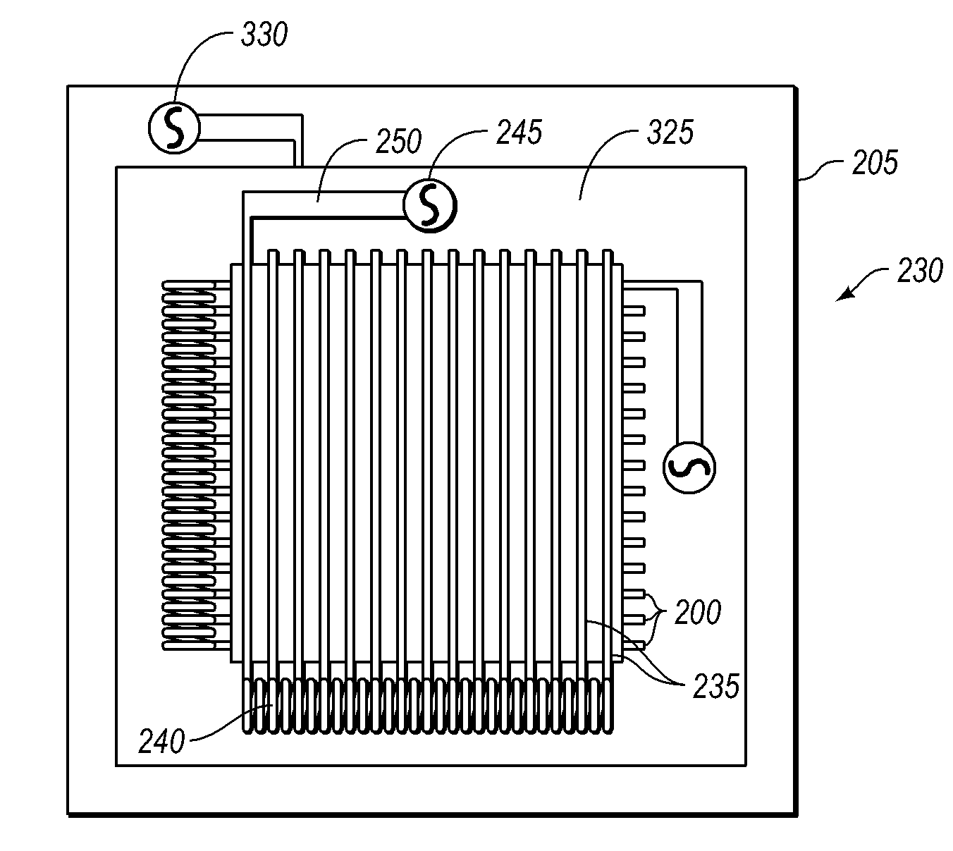
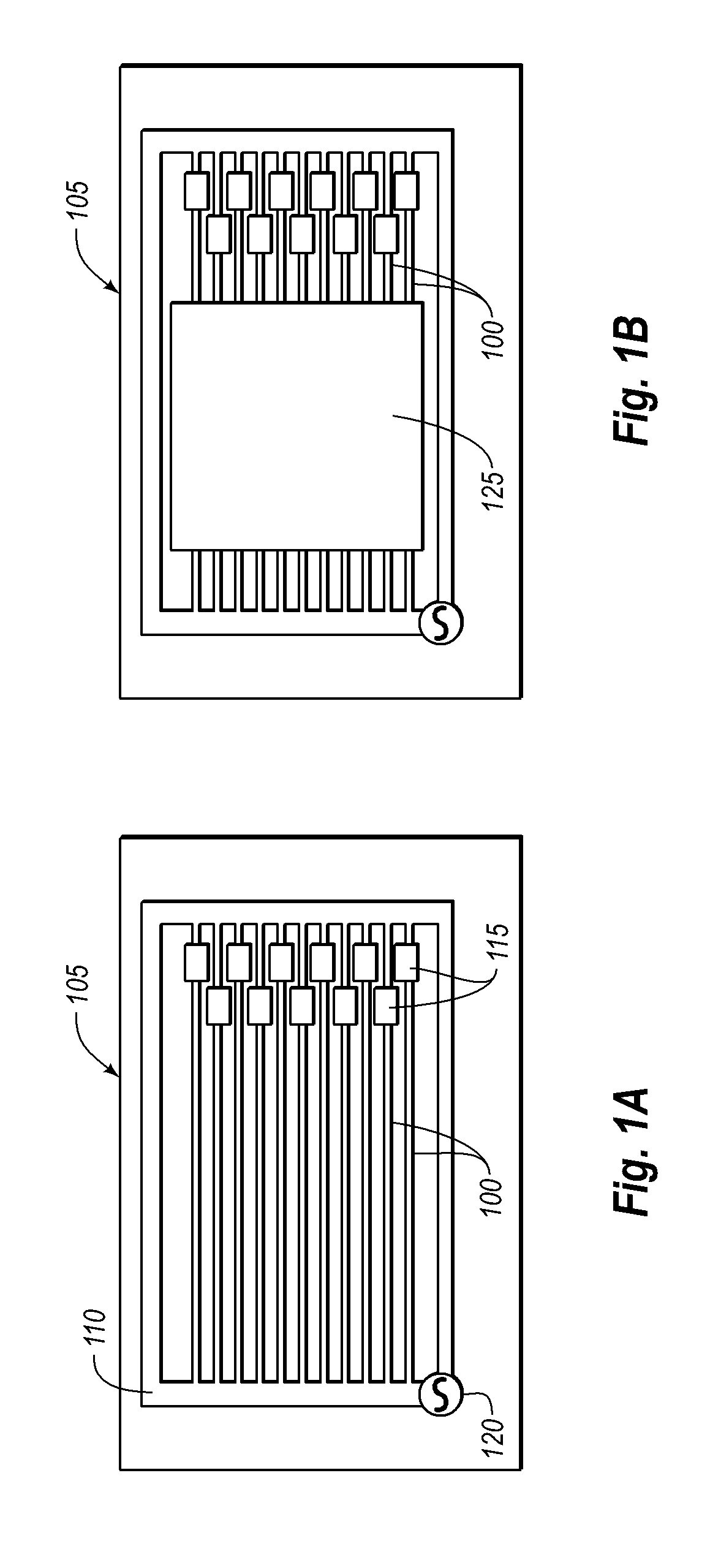
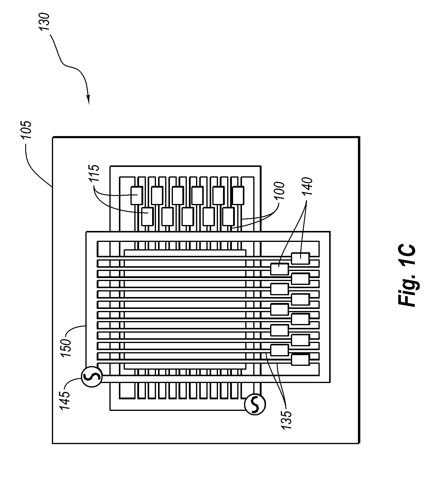
[0036]The principles of the embodiments disclosed herein describe the structure and operation of several examples used to illustrate the present invention. It should be understood that the drawings are diagrammatic and schematic representations of such example embodiments and, accordingly, are not limiting of the scope of the present invention, nor are the drawings necessarily drawn to scale. Well-known devices and processes have been excluded so as not to obscure the discussion in details that would be known to one of ordinary skill in the art.

[0037]Embodiments disclosed herein relate to simplifying and reducing the number of discrete traces used for addressing rows and columns in a matrix. The invention disclosed herein can exponentially reduce the conventional need for individual row and column drivers. In contrast to the relatively limiting and costly complex row and column constructs presently used in the industry, several embodiments can also reduce thickness. For example, som...


PUM

PropertyMeasurementUnit
wavelengthaaaaaaaaaa
frequenciesaaaaaaaaaa

Abstract

The present invention relates to displays including resonant trace structures. Displays are disclosed that include a first array of first electrically conductive traces configured to conduct alternating current, each of the first electrically conductive traces can be coupled to a first microelectromechanical system (MEM) surface acoustic wave (SAW) frequency selective filter. The displays further include a second array of second electrically conductive traces configured to conduct alternating current, each of the second electrically conductive traces can be coupled to a second microelectromechanical system (MEM) surface acoustic wave (SAW) frequency selective filter. The displays further include a material located between at least a portion of the first array and the second array, the material having a property that changes to cause illumination at points of intersection between the first array and the second array in response to current conducted in one or more of the first electrically conductive traces and current conducted in one or more of the second electrically conductive traces.

Description

CROSS-REFERENCE TO RELATED APPLICATIONS[0001]This application also the benefit of U.S. Provisional Patent Application Ser. No. 60 / 888,711, filed Feb. 7, 2007, claims the benefit of U.S. Provisional Patent Application Ser. No. 60 / 914,950, filed Apr. 30, 2007, and claims the benefit of U.S. Provisional Patent Application Ser. No. 61 / 022,303, filed Jan. 18, 2008. The contents of all of the aforementioned applications are incorporated by reference herein.BACKGROUND[0002]Dense circuit matrices typically contain row and column addressed integrated circuits. Addressing locations on dense circuit matrices are applicable to many different devices. For example, dense circuit matrices are often implemented in flat panel displays, charge-coupled devices (CCDs) such as digital cameras, deep space imagery from telescopes, microscopy, memory chips, electronic paper, heated pixel arrays, selective high density radio signal routing, and for selective curing of heat- or electro-sensitive materials. T...

Claims


Application Information

Patent Timeline
Patent Type & Authority Applications(United States)
IPC IPC(8): G02F1/1343G02F1/01G09G3/20H01J1/62
CPCG09G3/2096G09G2300/0426H01J9/02G09G2310/0267G09G2310/0275G09G2300/0439
Inventor MEISNER, MILTON D.
Owner MEISNER CONSULTING
Why Eureka
Try Eureka