Light-emitting device, illuminating device comprising same, and liquid crystal display
a technology of light-emitting devices and illuminating devices, which is applied in the direction of lighting support devices, lighting and heating apparatus, instruments, etc., can solve the problem of even larger regions, and achieve the effects of thin liquid crystal display, thin backlight, and low heigh
- Summary
- Abstract
- Description
- Claims
- Application Information
AI Technical Summary
Benefits of technology
Problems solved by technology
Method used
Image
Examples
first preferred embodiment
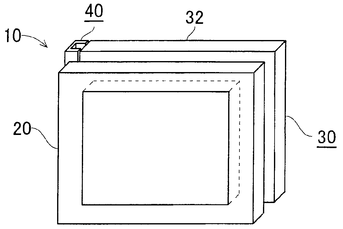
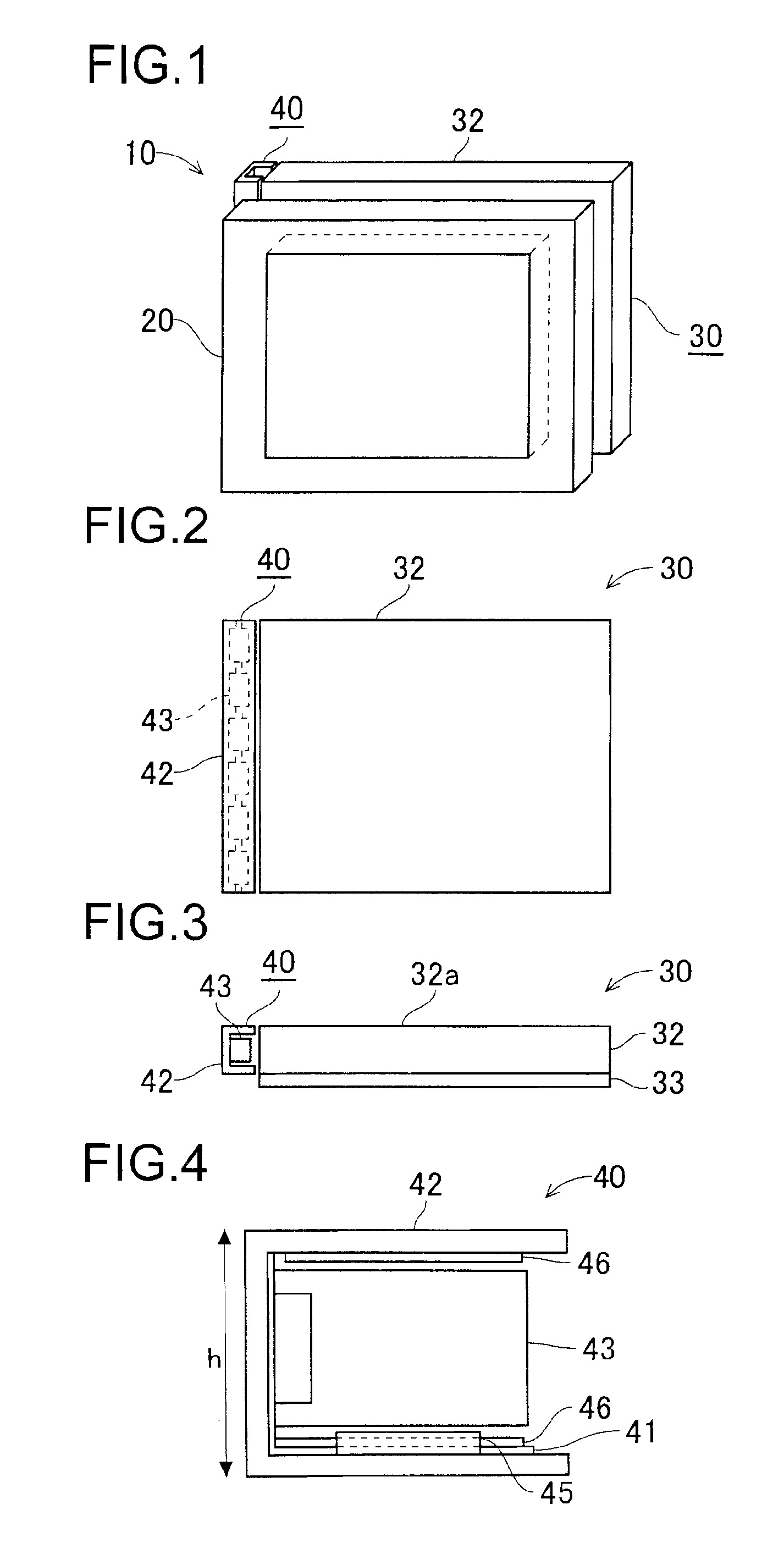
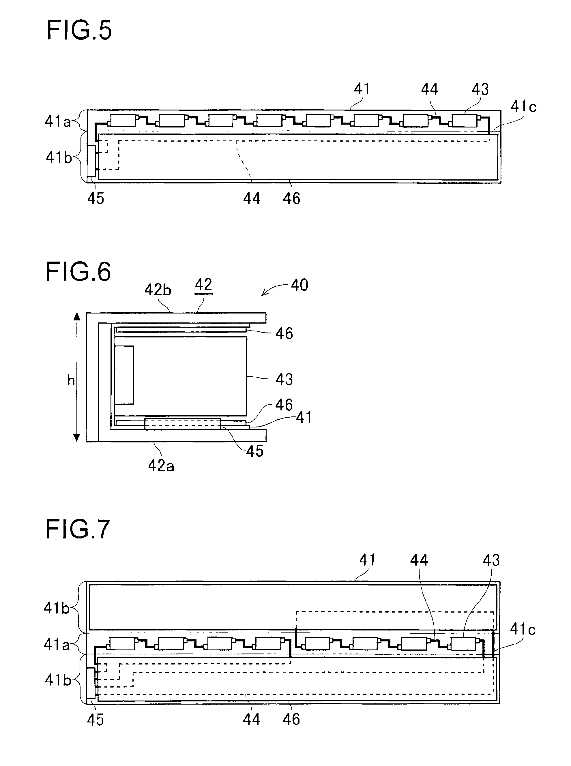
[0037]A description will be given of a first preferred embodiment of the present invention with reference to the accompanying drawings. FIG. 1 is a diagram schematically showing the structure of a liquid crystal display of the first preferred embodiment, FIG. 2 is a plan view showing a backlight of the first preferred embodiment, FIG. 3 is a front view showing the backlight, FIG. 4 is a front view showing a light-emitting device of the first preferred embodiment, and FIG. 5 is a developed view showing a film of the first preferred embodiment of the present invention.
[0038]As shown in FIG. 1, the liquid crystal display 10 is provided with a liquid crystal panel 20 and a backlight 30 that serves as an illuminating device. The liquid crystal panel 20 is provided with a TFT substrate, a counter substrate, and liquid crystal held between the TFT substrate and the counter substrate. The liquid crystal panel 20 displays an image by controlling the alignment of the liquid crystal by applyin...
second preferred embodiment
[0049]Next, a description will be given of a second preferred embodiment of the present invention with reference to the accompanying drawings. FIG. 9 is a developed view showing a film of the second preferred embodiment, and FIG. 10 is a front view of a light-emitting device of the second preferred embodiment. The second preferred embodiment has the same structure as the first preferred embodiment except that the LEDs are arranged on the film in a different manner, and the parts and components that are substantially the same as those in the first preferred embodiment are identified with the same reference numerals.
[0050]As shown in FIG. 9, a film 41 of this preferred embodiment is formed of a conductor region 41b and two LED mounting regions 41a between which the conductor region 41b is sandwiched. A plurality of LEDs 43, which are connected to one another by a conductor 44, are arranged on each of the LED mounting regions 41a. The conductors 44, no matter which one of the LED mount...
PUM
| Property | Measurement | Unit |
|---|---|---|
| conductor | aaaaa | aaaaa |
| length | aaaaa | aaaaa |
| structure | aaaaa | aaaaa |
Abstract
Description
Claims
Application Information


