
Nonvolatile storage device, memory controller, and defective region detection method

a nonvolatile storage device and memory controller technology, applied in error detection/correction, instruments, computing, etc., can solve the problems of single piece of memory cell that is difficult to keep its reliability, write and read error, and memory cell deterioration. , to achieve the effect of high possibility of error occurrence and highly reliable nonvolatile storage devi

Inactive Publication Date: 2009-02-26
PANASONIC INTELLECTUAL PROPERTY MANAGEMENT CO LTD
View PDF8 Cites 122 Cited by
  • Summary
  • Abstract
  • Description
  • Claims
  • Application Information

AI Technical Summary

Benefits of technology

The present invention relates to a method for reducing reading errors in nonvolatile storage devices such as memory cards. The invention detects physical blocks that are likely to have fixed defects or accumulated bit errors caused by reading, and provides a memory card with reduced reading errors. The invention aims to improve the reliability of nonvolatile storage devices by tolerating the existence of bit errors and continuing to use the flash memory through error correction.

Problems solved by technology

In the nonvolatile memory, however, memory cells gradually deteriorate every time data is rewritten, and finally, writing and reading errors will occur.
However, a single piece of the memory cell is difficult to keep its reliability due to miniaturization of a size of the memory cell by a process refinement and being multileveled for realizing a large capacity.
Since an area of memory patterns increases as the capacity thereof increases and time for a product inspection becomes long, sufficiently accurate inspection for the device becomes difficult.

Method used


Image

  • Nonvolatile storage device, memory controller, and defective region detection method
  • Nonvolatile storage device, memory controller, and defective region detection method
  • Nonvolatile storage device, memory controller, and defective region detection method

Examples


first embodiment

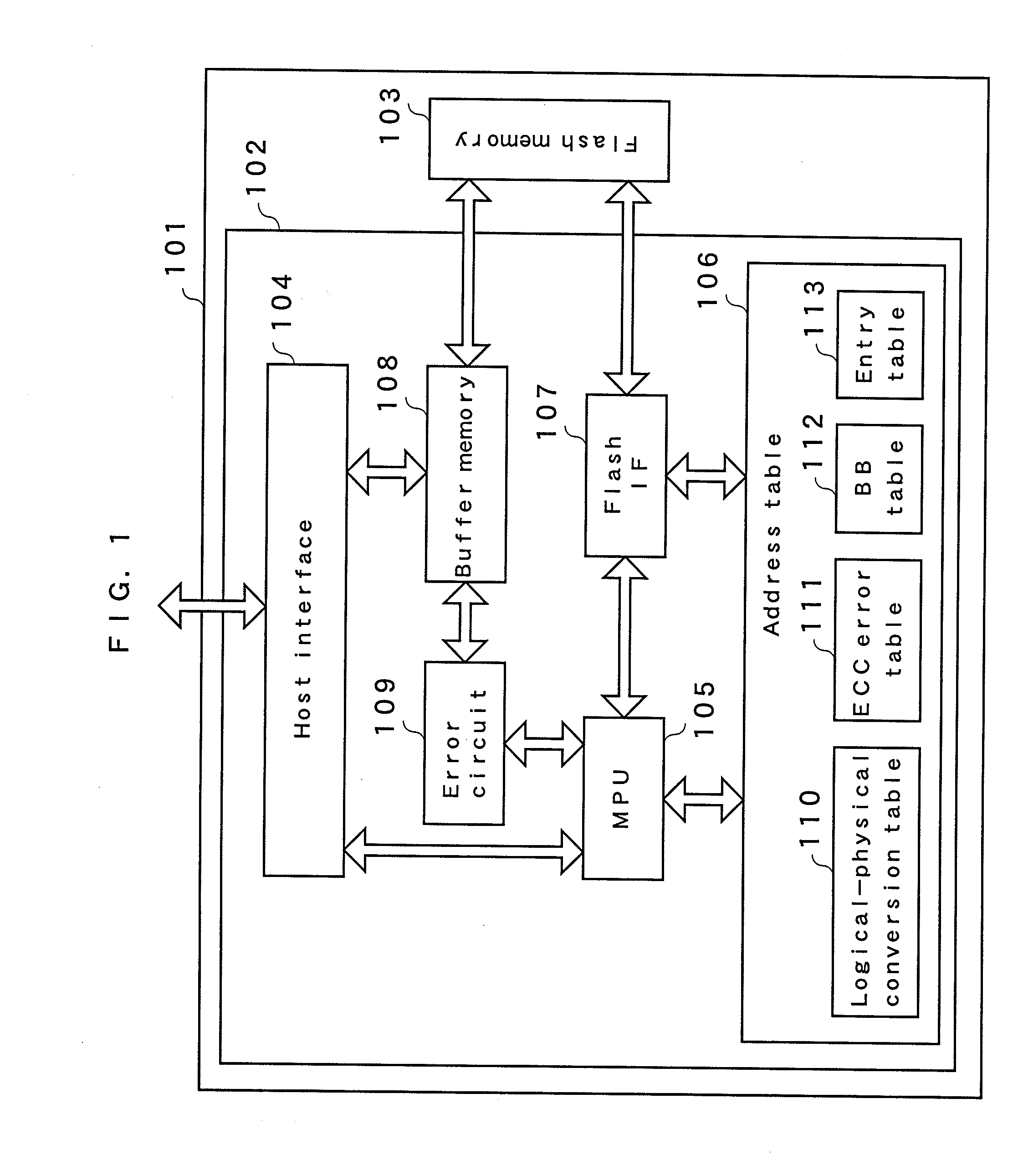
[0112]FIG. 1 is a block diagram showing a configuration of a nonvolatile storage device in a first embodiment. A memory card 101 includes a memory controller 102 and a flash memory 103 of a nonvolatile memory.

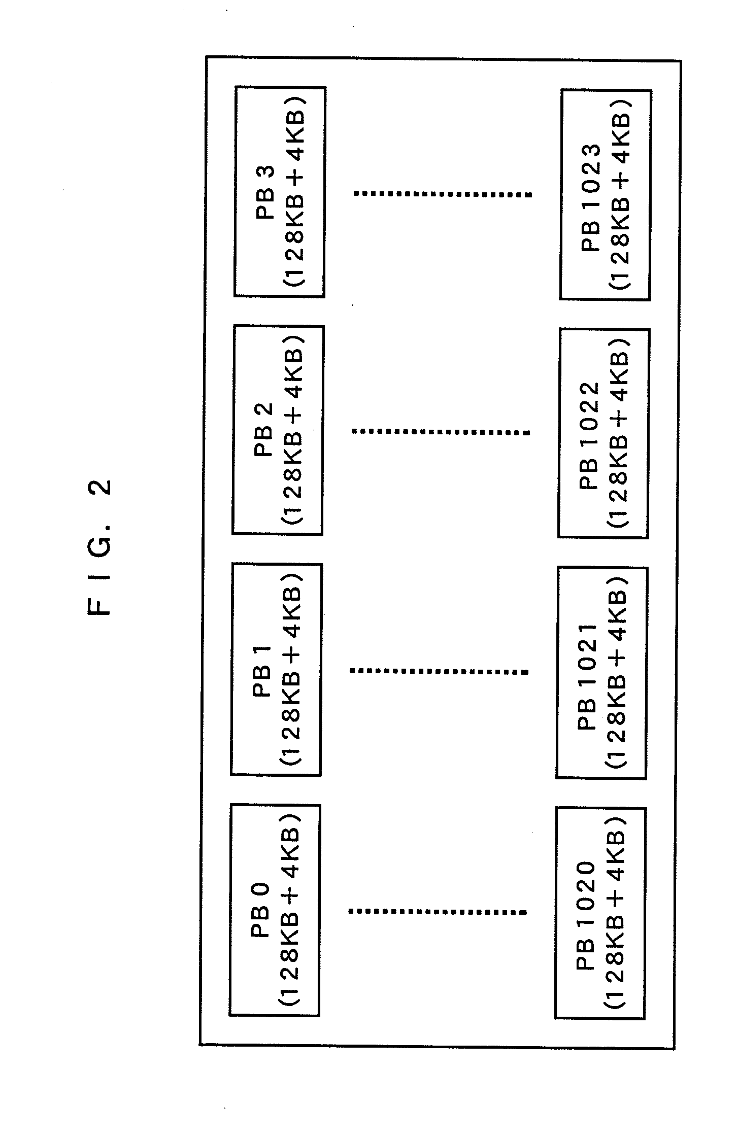
[0113]FIG. 2 is a block diagram showing an internal configuration of the flash memory 103. The flash memory having a size of 1 Gbits will be explained here. An inside of the flash memory 103 is composed of 1024 physical blocks of PB0 to PB1023. The physical block is a minimum unit for data erasing in the flash memory 103. A size of a physical block is 128 kB+4 kB, and the size has not a value of the power of 2 but a slightly larger size than the power of 2. The expression of 128 kB+4 kB, not 132 kB, means that a data size which can be written into one physical block is 128 kB and, in addition to this, management data such as an ECC code and a logical address of the physical block is further written into the area of 4 kB.

[0114]FIG. 3 is a block diagram showing an internal config...

second embodiment

[0139]FIG. 1 shows a configuration of the nonvolatile memory device according to the present embodiment. The memory card 101 includes the memory controller 102 and the flash memory 103 that is a nonvolatile memory. Respective components included in the memory controller 102 are the same as those explained in the first embodiment.

[0140]FIG. 2 is a view showing an internal configuration of the flash memory 103, the inside of the flash memory 103 includes 1024 physical blocks of PB 0 to PB 1023. FIG. 3 is a block diagram showing a configuration of the inside of a physical block, and respective blocks have 64 physical pages of PP0 to PP63. These are the same as those explained in the first embodiment.

[0141]The ECC error table 111 shown in FIG. 5 includes a plurality of the ECC error records #i, and is the same as that explained in the first embodiment.

[0142]FIG. 10 shows configuration of the ECC error records #i in the present embodiment. In FIG. 10, an error page 1001 is included in ad...

third embodiment

[0150]FIG. 1 shows a configuration of a nonvolatile memory device according to the present embodiment. The memory card 101 includes the memory controller 102 and the flash memory 103 that is a nonvolatile memory. Respective components included in the memory controller 102 are the same as those explained in the first embodiment.

[0151]FIG. 2 is a block diagram showing an internal configuration of the flash memory 103, inside of the flash memory 103 includes 1024 physical blocks of PB 0 to PB 1023. FIG. 3 is a block diagram showing a configuration of inside of a physical block, and respective physical blocks have 64 physical pages of PP0 to PP63. These are the same as those explained in the first embodiment.

[0152]The ECC error table 111 shown in FIG. 5 includes a plurality of the ECC error record #i, and is the same as that explained in the first embodiment.

[0153]FIG. 12 shows a configuration of the ECC error records #i in the present embodiment. FIG. 12 shows fields in the ECC error r...


PUM


Abstract

It is possible to accurately detect a physical block which has caused a fixture defect in a flash memory so as to limit the use of the physical block. By recording a history of generation of a physical block error and a history of physical erasing in an ECC error record, it is judged whether the error which has occurred is accidental or caused by a fixture defect. When no error is caused in the data written by physical erasing after a first read error occurrence, the first error is accidental and if another error is caused, the error is judged to be caused by a fixture defect. By using such an ECC error record, it is possible to accurately judge whether the error is accidental or caused by a fixture defect. By eliminating use of the physical block judged to have a fixture defect, it is possible to reduce read errors.

Description

TECHNICAL FIELD[0001]The present invention relates to a nonvolatile storage device, memory controller, and defective region detection method for reducing non accidental read errors generated by a defect of a nonvolatile memory, in the nonvolatile storage device using an error correcting function for improving reliability of data recorded in the nonvolatile memory.BACKGROUND ART[0002]A memory card mounting a nonvolatile memory expands its market as the memory card for a digital camera and a mobile phone. In the nonvolatile memory, however, memory cells gradually deteriorate every time data is rewritten, and finally, writing and reading errors will occur. Obviously, if the deterioration of the memory cells caused by the rewriting can be almost ignored because of sufficiently high reliability thereof, there will be no problem even in a usage for 10 years. It cannot be so actually, thus, by mounting an error correction circuit such as an ECC (Error Check and Correct) circuit on a system...

Claims


Application Information

Patent Timeline
Patent Type & Authority Applications(United States)
IPC IPC(8): G06F11/07
CPCG06F11/1068
Inventor HONDA, TOSHIYUKIMAKI, KUNIHIROKOGITA, SHIGEKAZU
Owner PANASONIC INTELLECTUAL PROPERTY MANAGEMENT CO LTD
Learn More