Automated systems and methods for adapting semiconductor fabrication tools to process wafers of different diameters

a technology of automatic systems and methods, applied in the field of semiconductor processing, can solve problems such as taking even longer

Inactive Publication Date: 2009-03-12
ADVANCED TECHNOLOGY DEVELOPMENT FACILITY +1
View PDF5 Cites 56 Cited by
  • Summary
  • Abstract
  • Description
  • Claims
  • Application Information

AI Technical Summary

Benefits of technology

[0008]In yet another embodiment, a method comprises providing a semiconductor fabrication tool comprising a stage heater having a plurality of wafer lifts, a baffle surrounding the stage heater and having a plurality of ring lifts, and an arm lift having a plurality of wafer lift pins and a plurality ring lift pins, the plurality of ring lift pins being aligned with the plurality of ring lifts and the plurality of wafer lift pins being aligned with the plurality of wafer lifts; moving the arm lift upward to cause the plurality of ring lift pins to rai

Problems solved by technology

However, due to the high costs involved in building 300 mm wafer fabrication plants from the ground up, many manufacturers have instead chosen to upgrade their e

Method used


Image

  • Automated systems and methods for adapting semiconductor fabrication tools to process wafers of different diameters
  • Automated systems and methods for adapting semiconductor fabrication tools to process wafers of different diameters
  • Automated systems and methods for adapting semiconductor fabrication tools to process wafers of different diameters

Examples


Embodiment Construction

[0020]In the following detailed description, reference is made to the accompanying drawings that illustrate embodiments of the present invention. These embodiments are described in sufficient detail to enable a person of ordinary skill in the art to practice the invention without undue experimentation. It should be understood, however, that the embodiments and examples described herein are given by way of illustration only, and not by way of limitation. Various substitutions, modifications, additions, and rearrangements may be made without departing from the spirit of the present invention. Therefore, the description that follows is not to be taken in a limited sense, and the scope of the present invention is defined only by the appended claims.

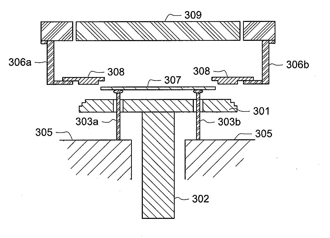
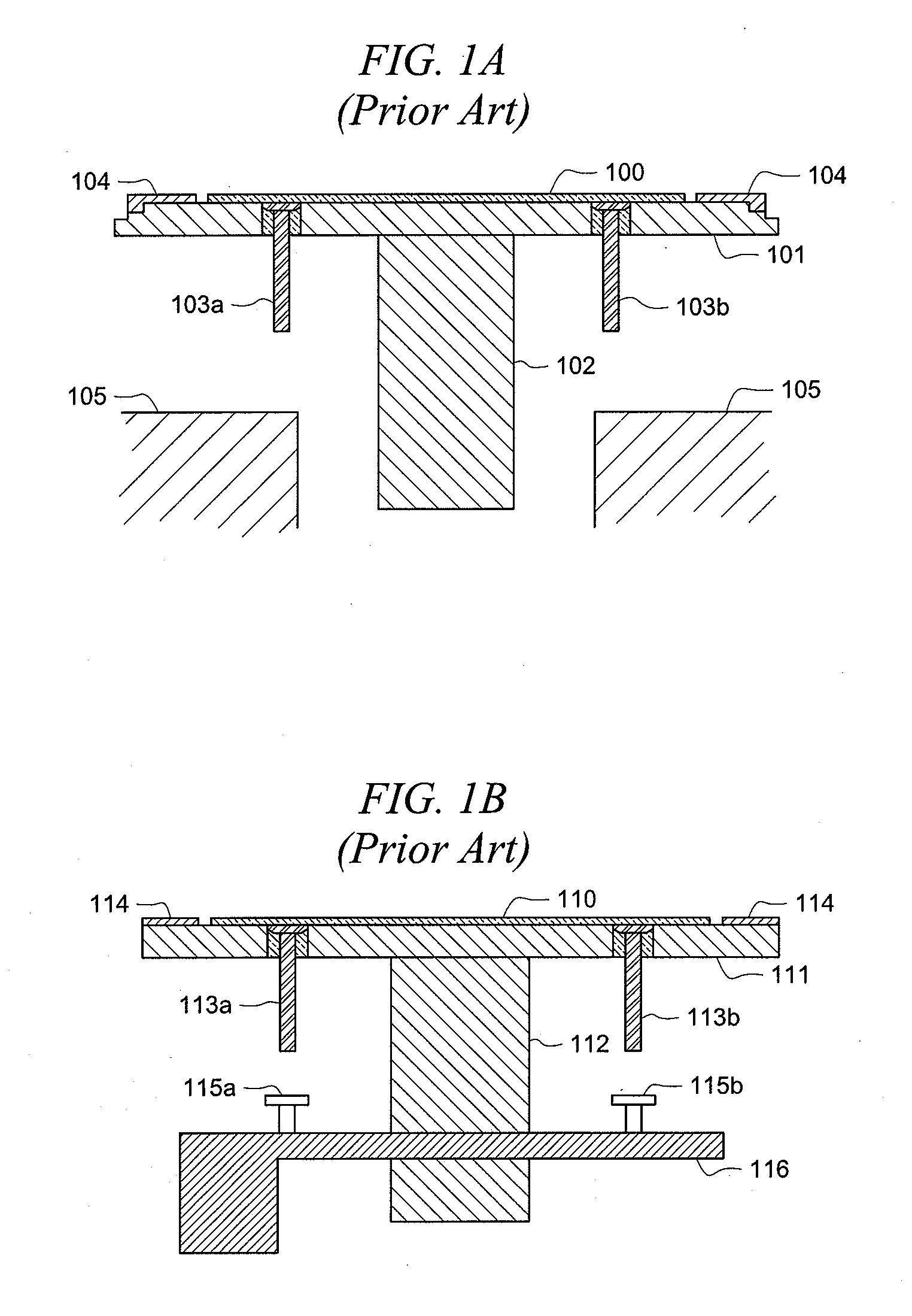
[0021]FIGS. 1A and B show cross-section views of prior art 300 mm semiconductor fabrication tools manually adaptable to process 200 mm wafers. Particularly, FIG. 1A shows 200 mm wafer 100 placed on stage heater 101 along with adapter ring 104...


PUM


Abstract

Automated systems and methods for adapting semiconductor fabrication tools to process wafers of different diameters are described. In one embodiment, a method comprises providing a semiconductor fabrication tool, placing an adapter ring on a plurality of ring holders via a robotic arm, the plurality of ring holders being operable to support the adapter ring at a vertical distance from a stage heater and the stage heater being movable in a vertical direction, placing a first semiconductor wafer on the stage heater via the robotic arm, the first semiconductor wafer having a first diameter, and moving the stage heater upward to receive the adapter ring from the plurality of ring holders and to cover a portion of the stage heater during processing of the first semiconductor wafer.

Description

BACKGROUND OF THE INVENTION[0001]1. Field of the Invention[0002]The present invention relates generally to semiconductor processing and, more particularly, to automated systems and methods for adapting semiconductor fabrication tools to process wafers of different diameters.[0003]2. Description of Related Art[0004]The semiconductor industry is subject to constant technological advances. One relatively recent improvement has been the introduction of 300 mm wafer processing. Manufacturing tools that had been fabricating integrated circuits on wafers having diameters of 200 mm are now in the process of being replaced with tools capable of processing 300 mm wafers. However, due to the high costs involved in building 300 mm wafer fabrication plants from the ground up, many manufacturers have instead chosen to upgrade their existing 200 mm tools to enable them to process 300 mm wafers. Accordingly, equipment suppliers currently offer 200 mm to 300 mm and 300 mm to 200 mm bridge tools or c...

Claims


Application Information

Patent Timeline
IPC IPC(8): H01L21/67
CPCH01L21/68742H01L21/68721
Inventor LANEE, KHAMSIDIMOORE, GERRY
Owner ADVANCED TECHNOLOGY DEVELOPMENT FACILITY
Why Eureka
Try Eureka