High speed multiple memory interface I/O cell

a memory interface and high-speed technology, applied in the field of memory interfacing, can solve the problem that there is no single solution that supports multiple memory interfaces, and achieve the effect of high speed

Inactive Publication Date: 2009-04-09
BROADCOM INT PTE LTD
View PDF4 Cites 16 Cited by
  • Summary
  • Abstract
  • Description
  • Claims
  • Application Information

AI Technical Summary

Problems solved by technology

No one solution exists that supports multiple memory interfaces.

Method used


Image

  • High speed multiple memory interface I/O cell
  • High speed multiple memory interface I/O cell
  • High speed multiple memory interface I/O cell

Examples


Embodiment Construction

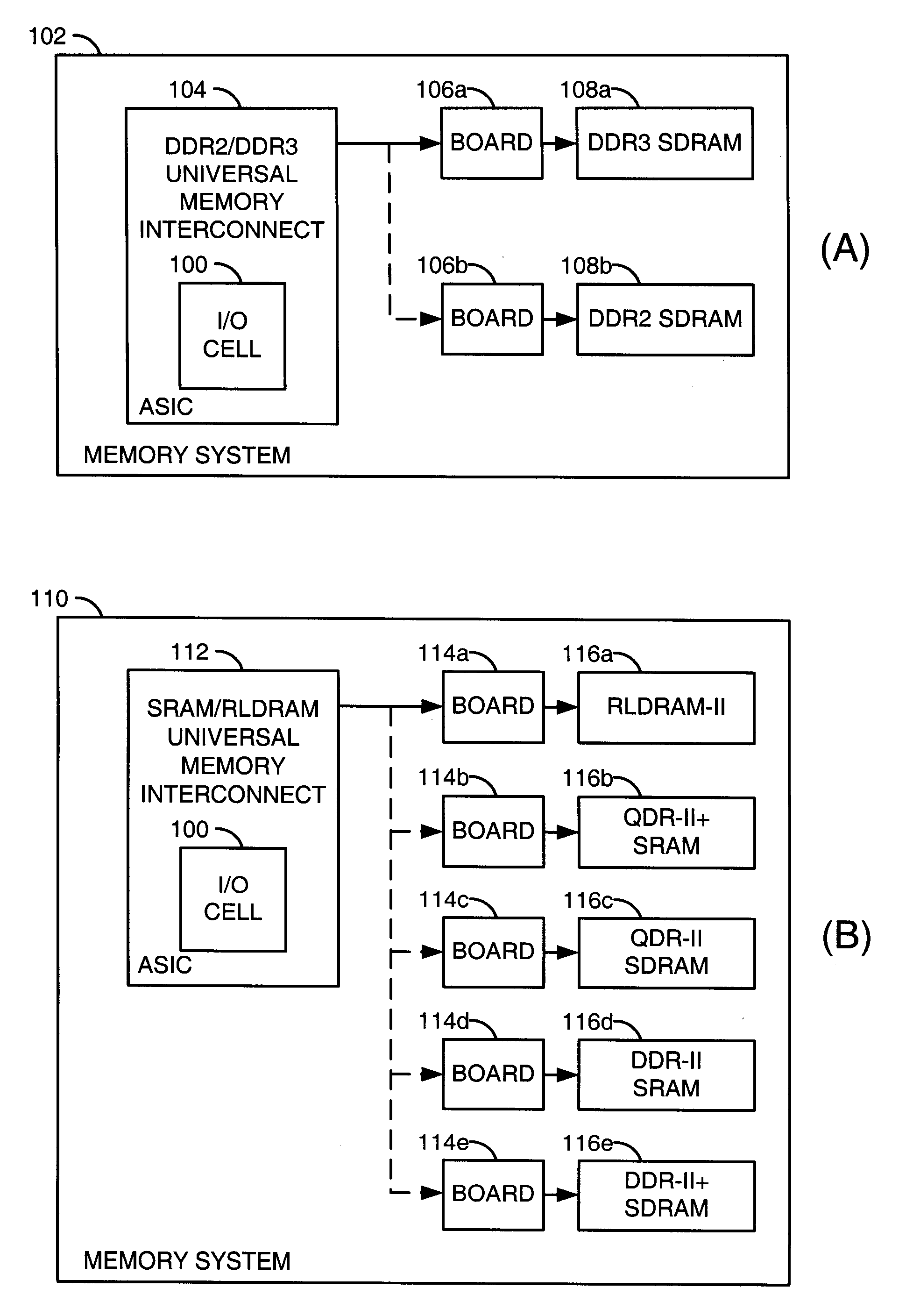
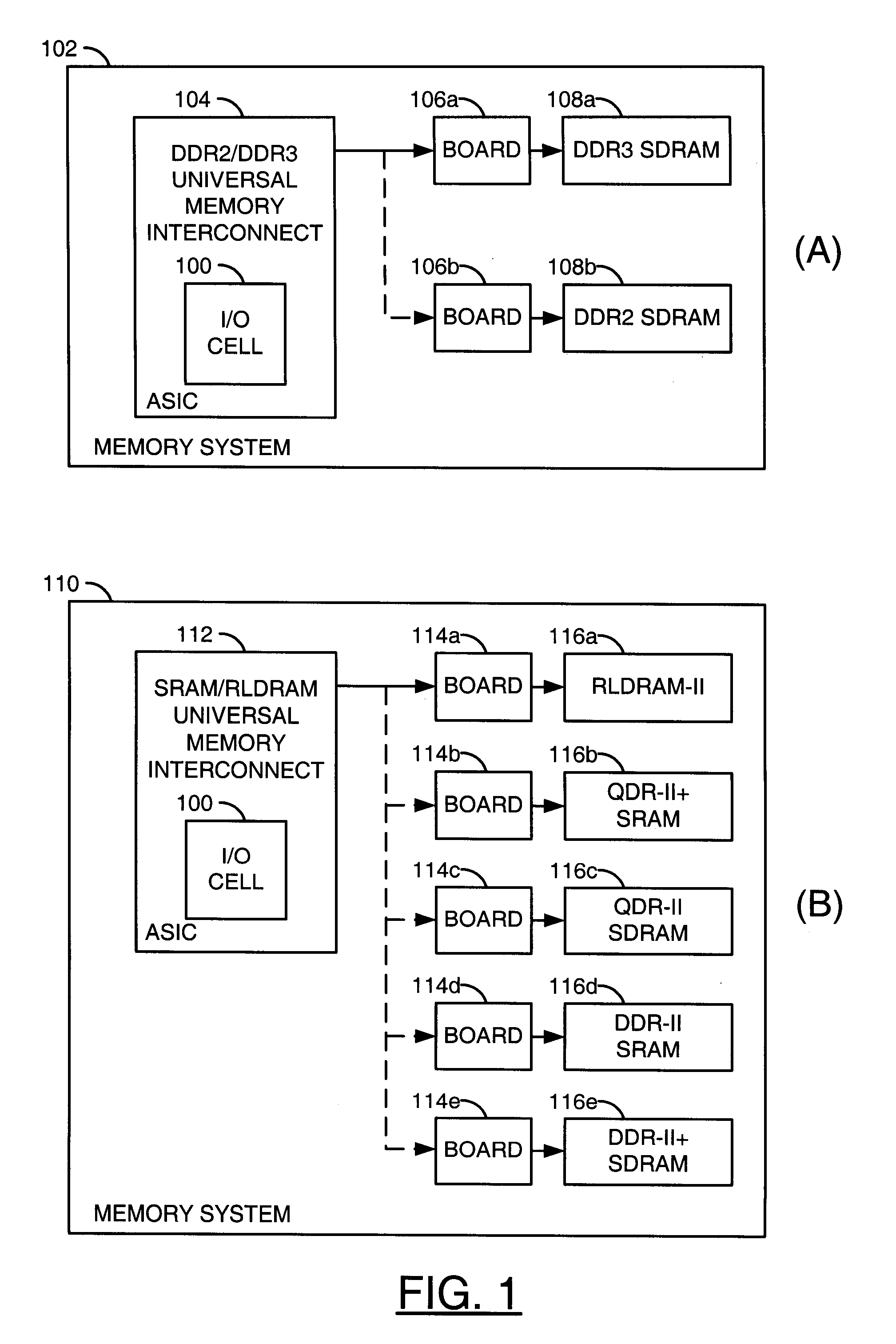
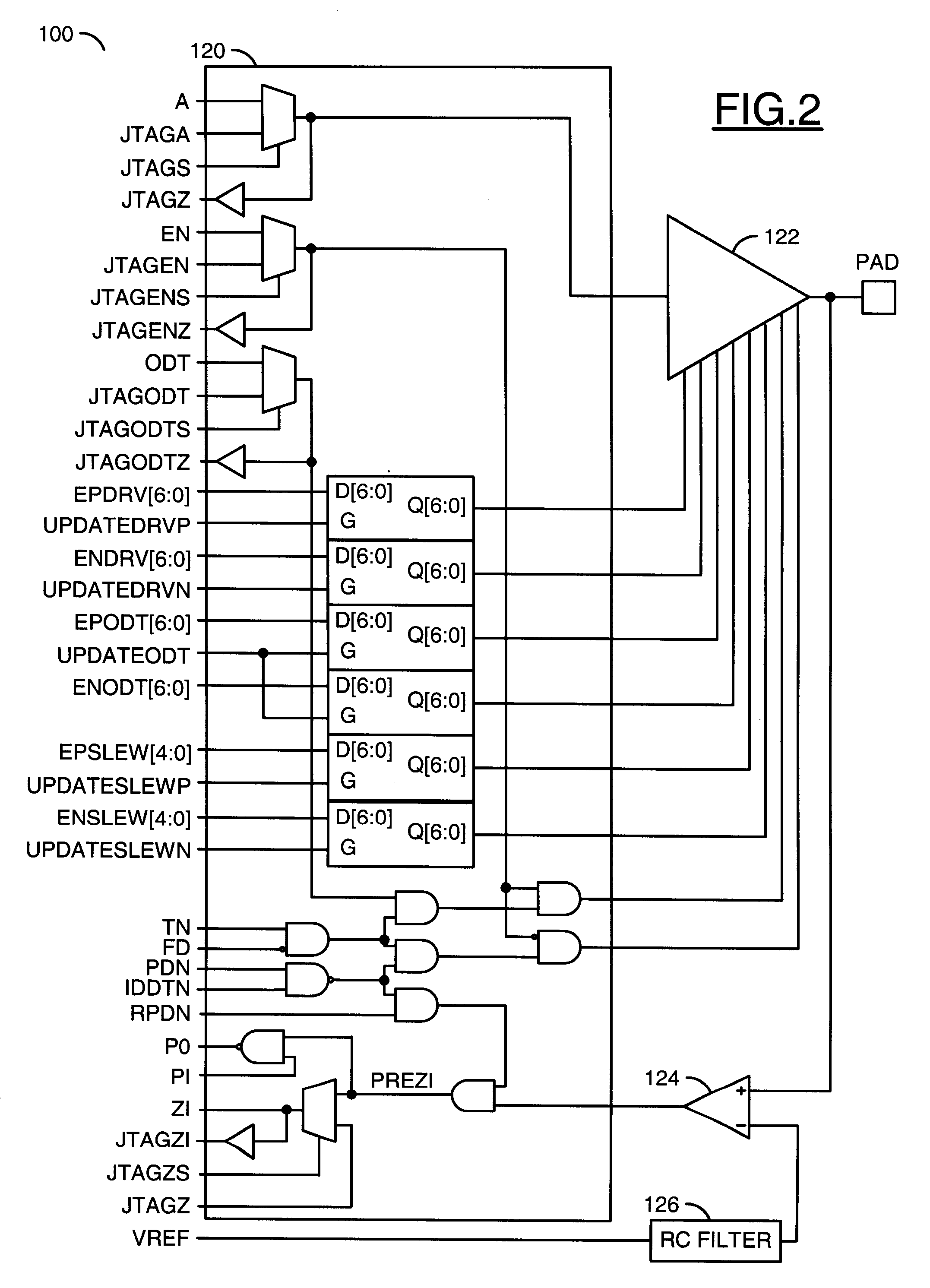
[0031]The present invention generally provides an input / output (I / O) cell that may programmed for compliance with multiple memory interface specifications (e.g., DDR2, DDR3, RLDRAM, SRAM, etc.). In one example, an I / O cell implemented in accordance with the present invention may provide a feature set that generally supports migration between DDR2, DDR3, RLDRAM, and / or SRAM memory interfaces.

[0032]Each memory interface specification generally has different I / O feature sets including specification of, for example, driver impedance, on-die termination impedance, I / O voltage levels, and slew rate as summarized in the following TABLES 1-4. Driver impedance ranges and tolerances of DDR2, DDR3, RLDRAM, and SRAM memory interfaces may be summarized in the following TABLE 1:

TABLE 1Supported DriverAdditionalImpedance Range (ohms)SpecificationsRLDRAM30 to 45Tolerance SRAM30 to 45Tolerance DDR2 SDRAM18 to 27Tolerance DDR3 SDRAM34 to 50Jedec Defined

On-die-termination (ODT) impedance ranges and to...


PUM


Abstract

An input / output (I / O) cell including one or more driver-capable segments and one or more on-die termination (ODT) capable segments. The I / O cell may be configured as an output driver in a first mode and Thevenin equivalent termination in a second mode.

Description

[0001]This application claims the benefit of U.S. Provisional Application Nos. 60 / 978,424 and 60 / 978,428, filed Oct. 9, 2007, and are hereby incorporated by reference in their entirety.FIELD OF THE INVENTION [0002]The present invention relates to memory interfacing generally and, more particularly, to a high speed multiple memory interface I / O cell.BACKGROUND OF THE INVENTION [0003]Separate input / output (I / O) solutions have been designed to support DDR2, DDR3, RLDRAM and SRAM memory interface specifications. No one solution exists that supports multiple memory interfaces. It would be desirable to have a solution that allows for interchangeability between DDR2 / DDR3 / RLDRAM / SRAM memory interfaces with one silicon solution.SUMMARY OF THE INVENTION [0004]In a first aspect, the present invention concerns an input / output (I / O) cell comprising (i) one or more driver-capable segments and (ii) one or more on-die termination (ODT) capable segments. In a second aspect, the present invention con...

Claims


Application Information

Patent Timeline
Patent Type & Authority Applications(United States)
IPC IPC(8): H03K19/003H03K19/0175G01R35/00
CPCG11C7/04G11C7/1045G11C7/1051G11C7/1057G11C7/1066G11C7/1069G11C2207/2254G11C29/022G11C29/028G11C29/50008G11C2029/5602G11C2207/105G11C29/02
Inventor BHAKTA, DHARMESHLIN, HONG-HIMKONG, CHENG-GANGRANDAZZO, TODD
Owner BROADCOM INT PTE LTD
Why Eureka
Try Eureka