LED array grid, method and device for manufacturing said grid and LED component for use in the same
- Summary
- Abstract
- Description
- Claims
- Application Information
AI Technical Summary
Benefits of technology
Problems solved by technology
Method used
Image


Examples
Embodiment Construction
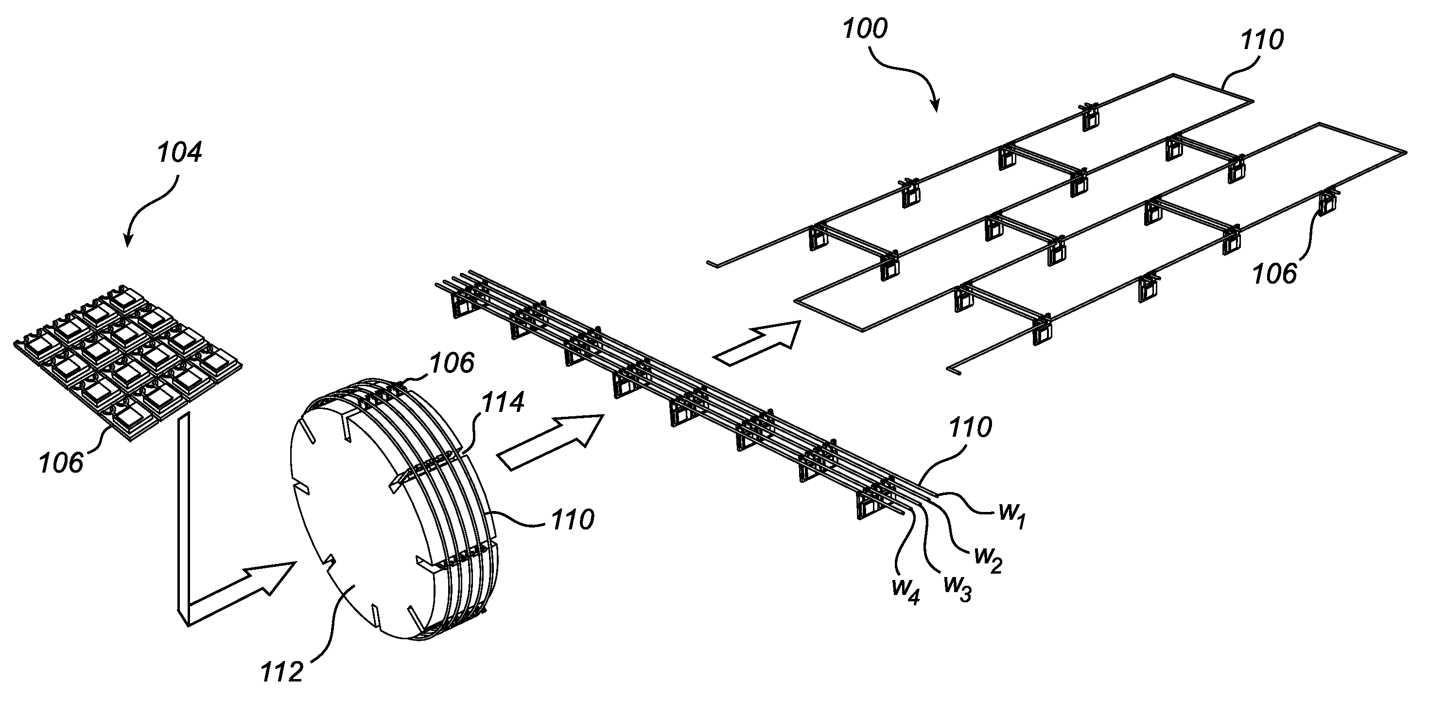
[0036]FIG. 1 shows the main steps of the inventive method. It illustrates an example of how LEDs 102 for use in the present invention can be arranged on a PCB 104, see also FIG. 2. The LEDs 102 can be prepackaged LEDs or naked dyes. In this example the PCB 104 is provided with a specific hole pattern and when the PCB 104 is diced into separate LED components 106 the holes 108 can be defined such as to provide attachment points used in a soldering process later on in the inventive method. It is cost efficient to arrange the LEDs 102 with a low pitch on a PCB 104 and to make as much use of the PCB material as possible.
[0037]After this preparing step the actual assembly takes place. A wire 110 is wound around an assembly drum 112, to be described in more detail later, and the separate LED components 106 are arranged in specific slots 114 that locates them before the wire 110 is wound into the holes 108 forming the attachment points. The wire is generally indicated with 110, while each ...
PUM
 Abstract
Description
Claims
Application Information