Design structure for chip identification system

Inactive Publication Date: 2009-04-09
GLOBALFOUNDRIES INC
View PDF9 Cites 12 Cited by
  • Summary
  • Abstract
  • Description
  • Claims
  • Application Information

AI Technical Summary

Benefits of technology

[0007]In view of the foregoing disclosed herein is a design structure of improved on-chip identification circuitry. The disclosed embodiments take advantage of across chip line variations (ACLV) and, optionally, random mask alignment variations to provide a unique on-chip identifier and/or a private key. In one embodiment, pairs of adjacent conductors (e.g., metal pads, vias, lines, etc.) are formed within one or more of the chip metallization layers. The distance between the conductors in each pair is predetermined so that, given known ACLVs, there will be a random chance (i.e., a 50% chance) that the conductors will short together. In another embodiment different masks can be used to form first conductors (e.g., metal lines separated by varying d

Problems solved by technology

Blowing fuses and/or anti-fuses at test increases testing time and, thereby, increases chip manufacturing costs.
Furthermore, these devices consume a relativel

Method used


Image

  • Design structure for chip identification system
  • Design structure for chip identification system
  • Design structure for chip identification system

Examples


Embodiment Construction

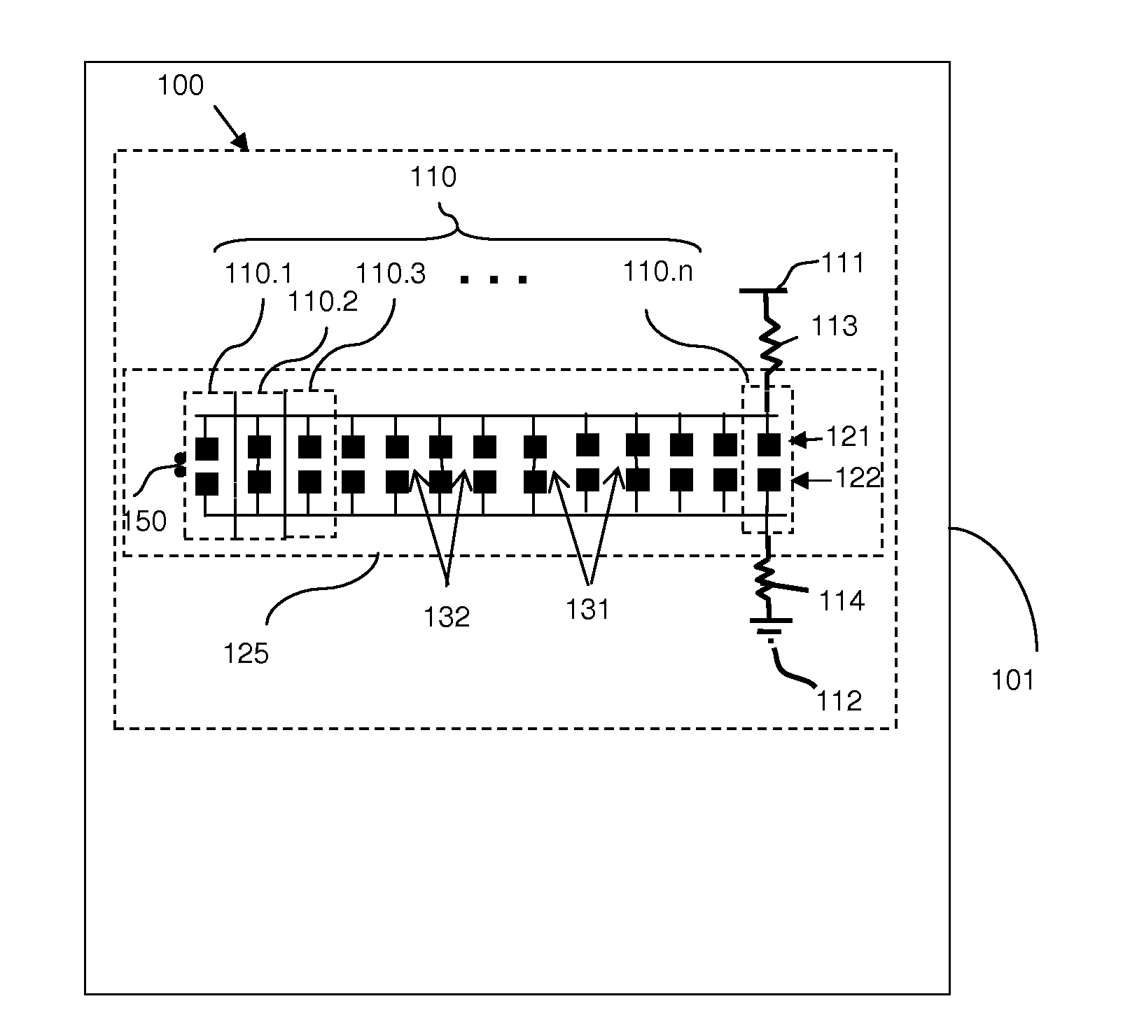
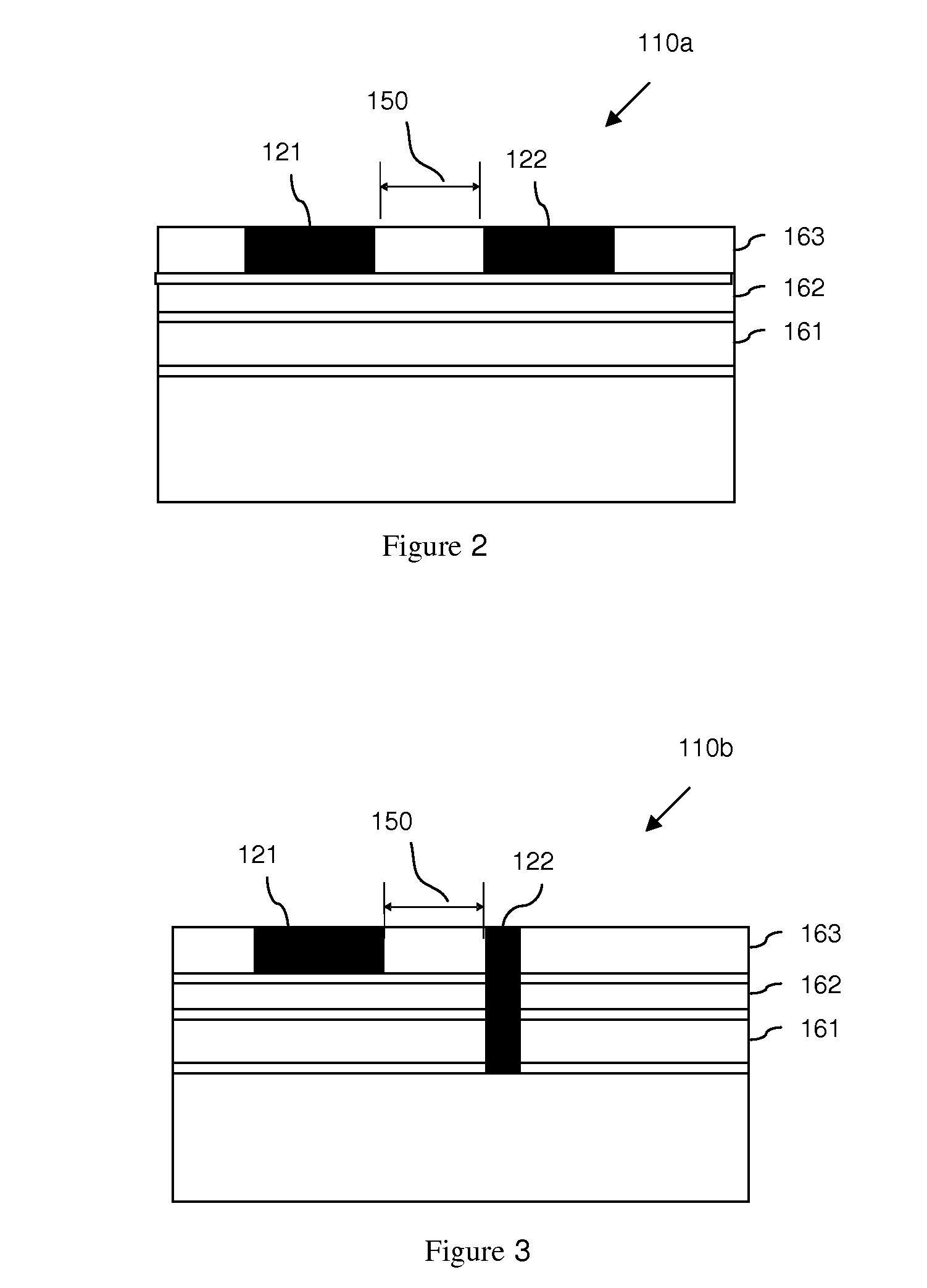
[0028]The embodiments of the invention and the various features and advantageous details thereof are explained more fully with reference to the non-limiting embodiments that are illustrated in the accompanying drawings and detailed in the following description. It should be noted that the features illustrated in the drawings are not necessarily drawn to scale. Descriptions of well-known components and processing techniques are omitted so as to not unnecessarily obscure the embodiments of the invention. The examples used herein are intended merely to facilitate an understanding of ways in which the embodiments of the invention may be practiced and to further enable those of skill in the art to practice the embodiments of the invention. Accordingly, the examples should not be construed as limiting the scope of the embodiments of the invention.

[0029]As mentioned above, integrated circuit chips often require unique on-chip identifiers. Typically, such identifiers are formed by providing...


PUM


Abstract

Disclosed is a design structure for an on-chip identification circuitry. In one embodiment, pairs of conductors (e.g., metal pads, vias, lines) are formed within one or more metallization layers. The distance between the conductors in each pair is predetermined so that, given known across chip line variations, there is a random chance (i.e., an approximately 50/50 chance) of a short. In another embodiment different masks form first conductors (e.g., metal lines separated by varying distances and having different widths) and second conductors (e.g., metal vias separated by varying distances and having equal widths). The first and second conductors alternate across the chip. Due to the different separation distances and widths of the first conductors, the different separation distances of the second conductors and, random mask alignment variations, each first conductor can short to up to two second conductors. In each embodiment the resulting pattern of shorts and opens, can be used as an on-chip identifier or private key.

Description

CROSS-REFERENCE TO RELATED APPLICATIONS [0001]This application is a Continuation-In-Part of U.S. application Ser. No. 11 / 869,179 filed Oct. 9, 2007, the complete disclosure of which, in its entirety, is herein incorporated by reference.BACKGROUND[0002]1. Field of the Invention[0003]The embodiments of the invention generally relate to a design structure, and more specifically, to a design structure for on-chip identification circuitry and improved on-chip identification circuitry that does not incorporate fuses and / or anti-fuses.[0004]2. Description of the Related Art[0005]Integrated circuit chips often require unique on-chip identifiers. Typically, such identifiers are formed by providing on-chip fuses and / or anti-fuses, which are programmed (i.e., blown) at test. Blowing fuses and / or anti-fuses at test increases testing time and, thereby, increases chip manufacturing costs. Furthermore, these devices consume a relatively large amount of chip space (e.g., approximately 7.3 μm2). Thu...

Claims


Application Information

Patent Timeline
IPC IPC(8): G06F17/50
CPCG06K19/067
Inventor BUETI, SERAFINOCOURCHESNE, ADAM J.GOODNOW, KENNETH J.LEONARD, TODD E.SANDON, PETER A.TWOMBLY, PETER A.WOODRUFF, CHARLES S.
Owner GLOBALFOUNDRIES INC
Why Eureka
Try Eureka