
Built-in self repair circuit for a multi-port memory and method thereof

a multi-port memory and self-repair technology, applied in the field of built-in self-repair circuits for multi-port memory, can solve the problems of increasing the complexity of circuit layout, affecting the accuracy of multi-port memory repair, and occupying a lot of chips, so as to avoid inaccurate or incomplete repairs to multi-port memory.

Inactive Publication Date: 2009-04-16
FARADAY TECH CORP
View PDF5 Cites 7 Cited by
  • Summary
  • Abstract
  • Description
  • Claims
  • Application Information

AI Technical Summary

Benefits of technology

[0012]Accordingly, the present invention is directed to a built-in self repair (BISR) circuit for a multi-port memory, wherein accurate and complete defect locations are provided based on fault locations detected by the BISR circuit so that incorrect or incomplete repairs to the multi-port memory can be avoided.
[0013]The present invention is directed to a BISR method for a multi-port memory, wherein accurate and complete defect locations in the multi-port memory are provided so that inaccurate or incomplete repairs to the multi-port memory and waste of redundancy element are avoided and accordingly the production yield is improved.
[0018]In the present invention, defects which cause port-specific faults are categorized and a specific locating process is executed corresponding to each defect category, and the corresponding defect location can be obtained based on the fault generated in the locating process. Accordingly, in the present invention, accurate and complete defect locations can be provided based on seeming fault locations so that inaccurate or incomplete repairs to a multi-port memory can be avoided.

Problems solved by technology

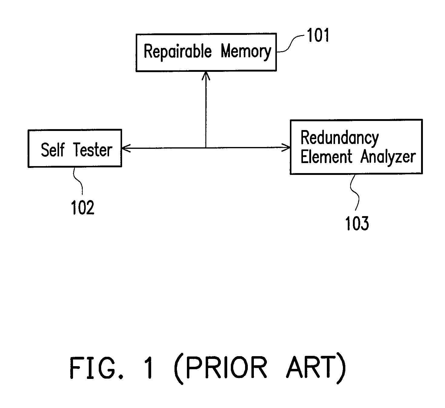
When an on-chip circuit contains multiple memories, testing of these memories will become a big problem.
All the input and output terminals of the memories have to be connected out of the chip if an external device is used for testing the memories, such an enormous circuit layout not only takes up a lot of chip surface and increases the complexity of the circuit layout but is unrealistic with only limited number of chip pins.
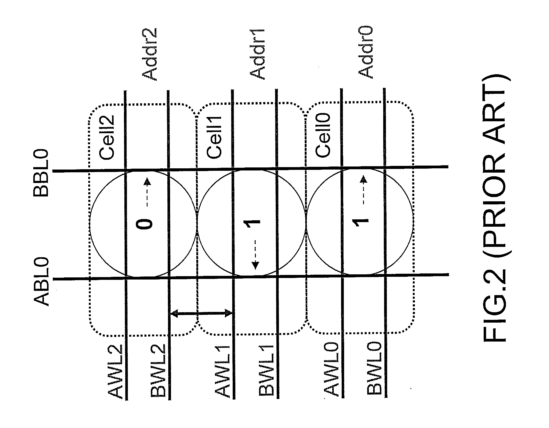
In this case, the actual defect cannot be repaired by repairing the faulty row, and it will also be a waste of the redundancy element and cause a yield loss.
Accordingly, even though a general testing algorithm can provide correct defect locations, the defect locations may not be complete.
Accordingly, a general testing algorithm provides incorrect location information of defects between word lines and insufficient location information of defects between bit lines.

Method used


Image

  • Built-in self repair circuit for a multi-port memory and method thereof
  • Built-in self repair circuit for a multi-port memory and method thereof
  • Built-in self repair circuit for a multi-port memory and method thereof

Examples


Embodiment Construction

[0031]Reference will now be made in detail to the present preferred embodiments of the invention, examples of which are illustrated in the accompanying drawings. Wherever possible, the same reference numbers are used in the drawings and the description to refer to the same or like parts.

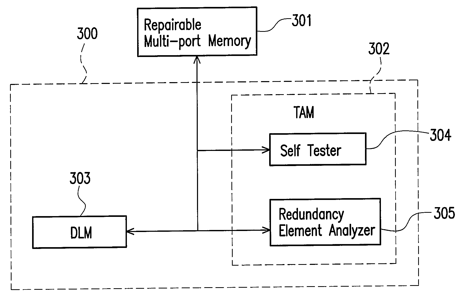
[0032]Please refer to FIG. 3 and FIG. 4 for following description. FIG. 3 is a diagram of a BISR circuit 300 for a multi-port memory according to an embodiment of the present invention, and FIG. 4 is a flowchart illustrating a BISR method for a multi-port memory executed by the BISR circuit 300. The BISR circuit 300 includes a test-and-analysis module (TAM) 302 and a defect locating module (DLM) 303, and the TAM 302 further includes a self tester 304 and a redundancy element analyzer 305. The repairable multi-port memory 301, the self tester 304, the redundancy element analyzer 305, and the DLM 303 are coupled to each other.

[0033]The procedure of FIG. 4 starts from step 405. In step 405, the self tes...


PUM


Abstract

A built-in self repair (BISR) circuit for a multi-port memory and a method thereof are provided. The circuit includes a test-and-analysis module (TAM) and a defect locating module (DLM) coupled to the TAM. The TAM tests a repairable multi-port memory to generate a fault location and determines whether the test generates a port-specific fault candidate according to the fault location. If a port-specific fault candidate is generated, the DLM generates a defect location based on the fault location and provides the defect location to the TAM so that the TAM can determine how to repair the repairable multi-port memory according to the defect location. If no port-specific fault candidate is generated in the test, the TAM determines how to repair the repairable multi-port memory according to the fault location.

Description

BACKGROUND OF THE INVENTION[0001]1. Field of the Invention[0002]The present invention generally relates to a built-in self repair (BISR) circuit for a memory and a method thereof, in particular, to a BISR circuit for a multi-port memory and a method thereof.[0003]2. Description of Related Art[0004]When an on-chip circuit contains multiple memories, testing of these memories will become a big problem. All the input and output terminals of the memories have to be connected out of the chip if an external device is used for testing the memories, such an enormous circuit layout not only takes up a lot of chip surface and increases the complexity of the circuit layout but is unrealistic with only limited number of chip pins. Thus, a concept of built-in self test (BIST) is provided, which is to fabricate a testing circuit and the memories to be tested on the same chip so that the input and output terminals of the memories do not have to be connected out of the chip for merely testing purpo...

Claims


Application Information

Patent Timeline
IPC IPC(8): G11C29/12
CPCG11C8/16G11C29/808G11C29/4401G11C29/44
Inventor TSENG, TSU-WEIHUANG, YU-JENWU, CHUN-HSIENLI, JIN-FUPAO, CHIEN-YUAN
Owner FARADAY TECH CORP
Learn More