Methods of Manufacturing Semiconductor Devices Having Contact Plugs in Insulation Layers

a technology of contact plugs and semiconductor devices, which is applied in the direction of semiconductor/solid-state device manufacturing, basic electric elements, electric devices, etc., can solve the problems of affecting the performance and affecting the reliability of semiconductor devices, so as to improve the contact reliability of bit line contact plugs and reduce current leakage.

Active Publication Date: 2009-04-23
SAMSUNG ELECTRONICS CO LTD
View PDF3 Cites 10 Cited by
  • Summary
  • Abstract
  • Description
  • Claims
  • Application Information

AI Technical Summary

Benefits of technology

[0010]Pursuant to embodiments of the present invention, methods of manufacturing semiconductor devices having contact plug st

Problems solved by technology

With the increase of the integration level of semiconductor devices, electrical insulation between metal lines such as bit lines and/or between metal lines and semiconductor layers may significantly affect the performance and reliability of a semiconductor device.
As the integration level of semiconductor devices has in

Method used


Image

  • Methods of Manufacturing Semiconductor Devices Having Contact Plugs in Insulation Layers
  • Methods of Manufacturing Semiconductor Devices Having Contact Plugs in Insulation Layers
  • Methods of Manufacturing Semiconductor Devices Having Contact Plugs in Insulation Layers

Examples


Embodiment Construction

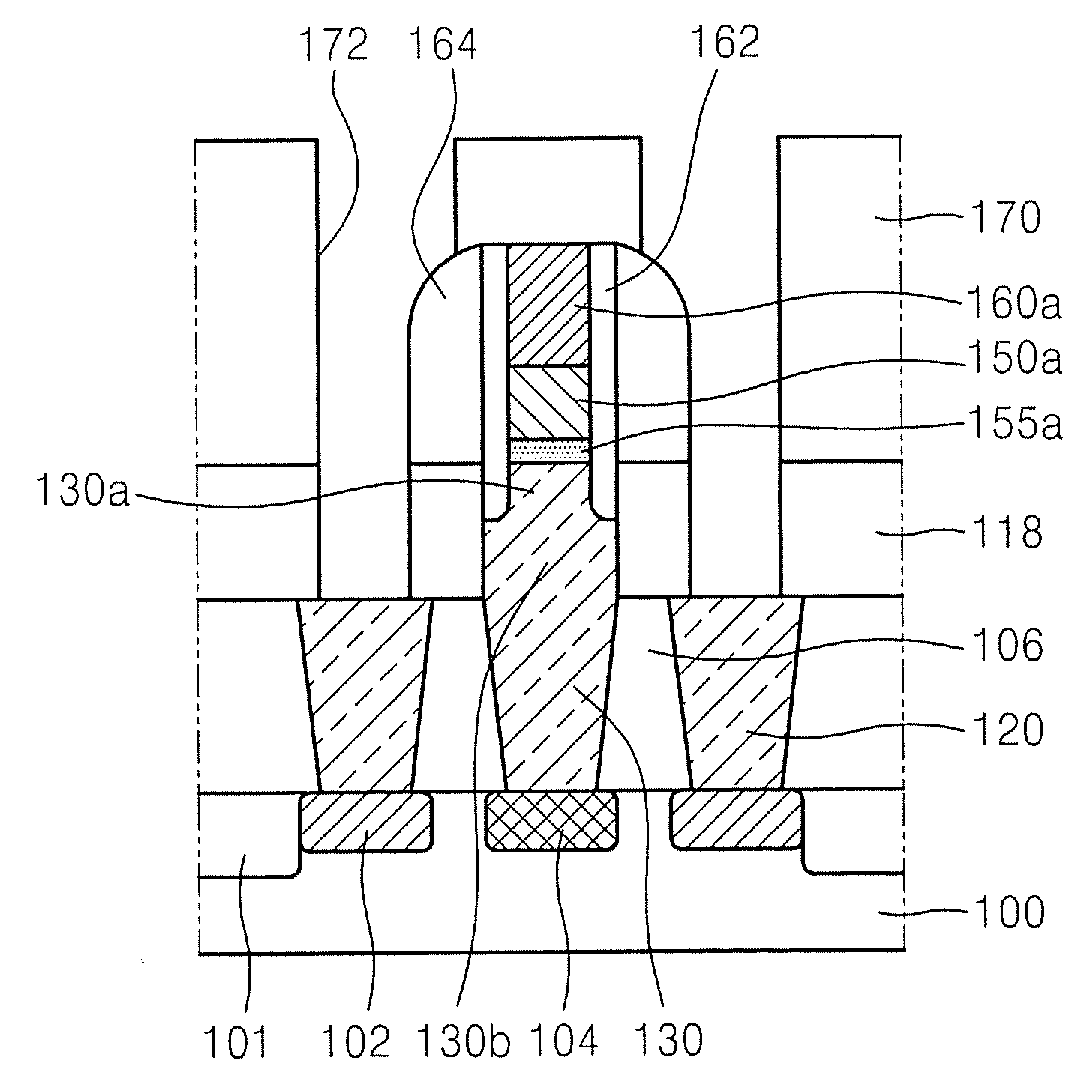
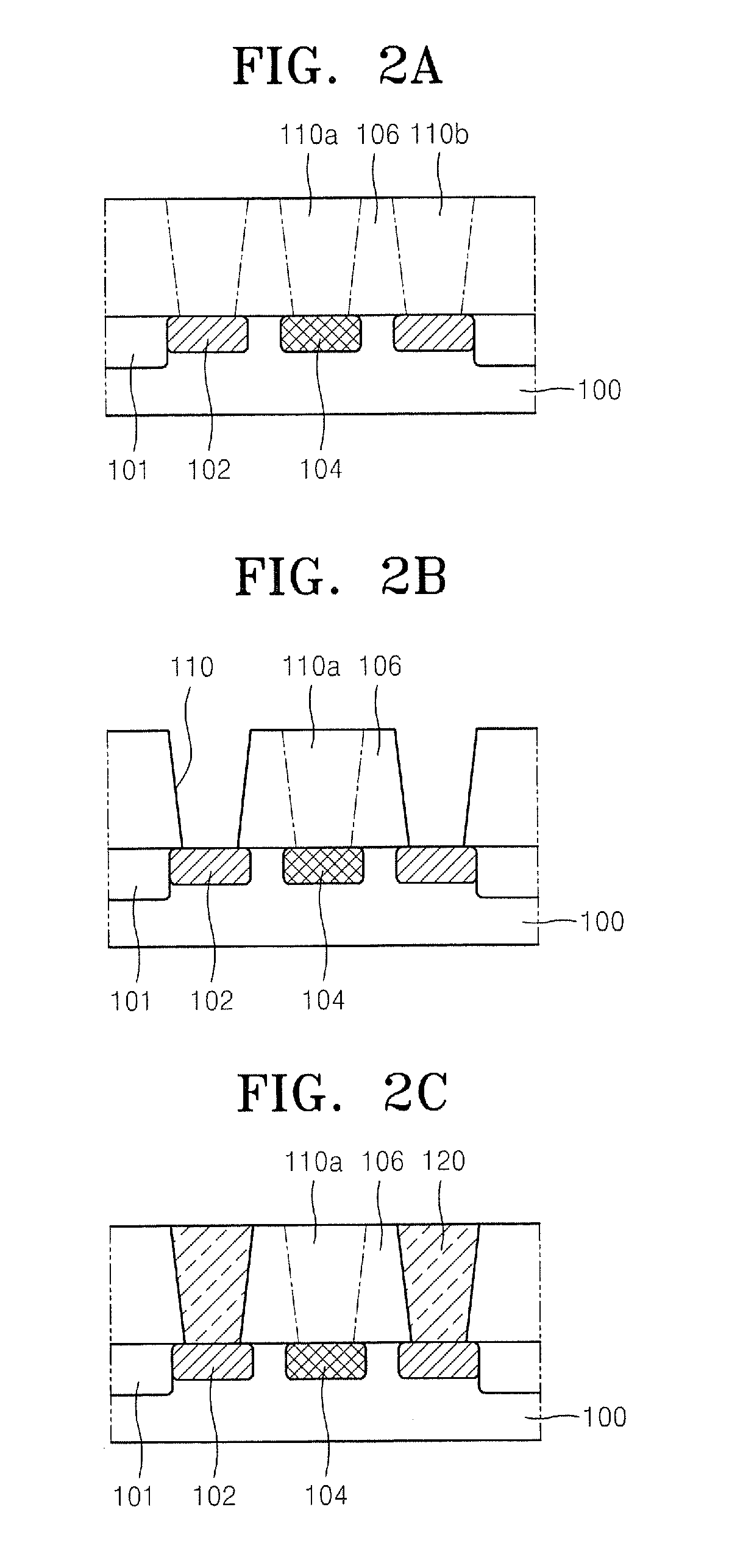
[0026]The present invention will now be described more fully with reference to the accompanying drawings, in which exemplary embodiments of the invention are shown. It will be appreciated, however, that the example embodiments illustrated herein are exemplary in nature and are not intended to be limiting. In the drawings, the thicknesses of layers and regions may be exaggerated for clarity.

[0027]It will be understood that when an element, such as a layer, a region, or a substrate, is referred to as being “on,”“connected to” or “coupled to” another element, it may be directly on, connected or coupled to the other element or intervening elements may be present. In contrast, when an element is referred to as being “directly on,”“directly connected to” or “directly coupled to” another element or layer, there are no intervening elements or layers present. Like reference numerals refer to like elements throughout. As used herein, the term “and / or” includes any and all combinations of one ...


PUM


Abstract

Methods of manufacturing semiconductor devices are provided in which a first contact plug is formed on a first active region in a substrate and a second contact plug is formed on a second active region in the substrate. A height of an upper surface of the second contact plug from the substrate is greater than a height of an upper surface of the first contact plug from the substrate. A third contact plug is formed on the second contact plug. A first spacer is formed on a side surface of the third contact plug. A third interlayer insulation layer is formed that covers the third contact plug. The third interlayer insulation layer is patterned to form a third opening that exposes the first contact plug. A fourth contact plug is formed in the third opening that is electrically connected to the first contact plug.

Description

CROSS-REFERENCE TO RELATED PATENT APPLICATION[0001]This application claims priority under 35 U.S.C. § 119 from Korean Patent Application No. 10-2007-0106740, filed on Oct. 23, 2007 in the Korean Intellectual Property Office, the disclosure of which is incorporated herein in its entirety by reference.FIELD OF THE INVENTION[0002]The present invention relates to semiconductor devices and, more particularly, to methods of manufacturing semiconductor devices having contact plug structures.BACKGROUND OF THE INVENTION[0003]With the increase of the integration level of semiconductor devices, electrical insulation between metal lines such as bit lines and / or between metal lines and semiconductor layers may significantly affect the performance and reliability of a semiconductor device. As the integration level of semiconductor devices has increased, it has become more difficult to provide a sufficient process margin when forming a contact pad that is used to connect a transistor to a metal li...

Claims


Application Information

Patent Timeline
IPC IPC(8): H01L21/02H01L21/4763
CPCH01L21/76897H01L21/76885H10B12/0335H10B12/482H10B12/485H01L21/28
Inventor SUNG, JOON-HOLEE, JU-YONGPARK, MI-KYUNGCHUNG, TAE-YOUNG
Owner SAMSUNG ELECTRONICS CO LTD
Why Eureka
Try Eureka