Semiconductor device having increased active region width and method for manufacturing the same

Inactive Publication Date: 2009-04-30
SK HYNIX INC
View PDF1 Cites 10 Cited by
  • Summary
  • Abstract
  • Description
  • Claims
  • Application Information

AI Technical Summary

Benefits of technology

[0007]Embodiments of the present invention are directed to a semiconductor device and a method for m

Problems solved by technology

However, in the conventional art, it is difficult to secure a gap-fill margin, because the gap-fill process is conducted after defining the trenches so as to form the isolation structure.
In addition, in the

Method used


Image

  • Semiconductor device having increased active region width and method for manufacturing the same
  • Semiconductor device having increased active region width and method for manufacturing the same
  • Semiconductor device having increased active region width and method for manufacturing the same

Examples


Example

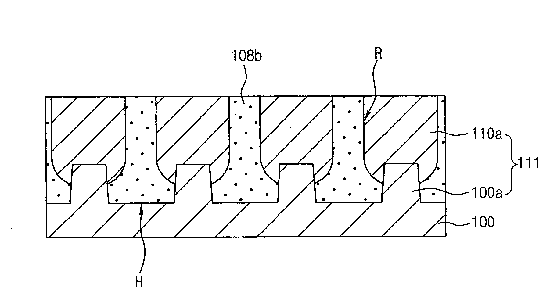
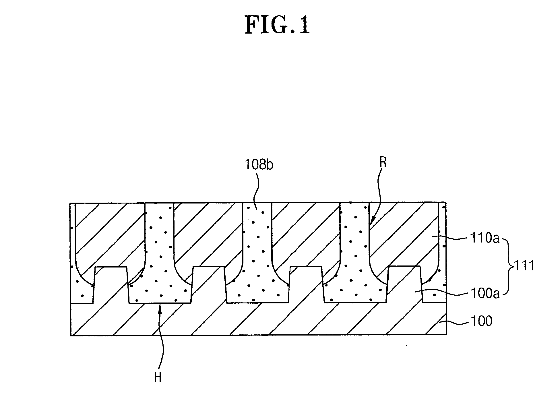
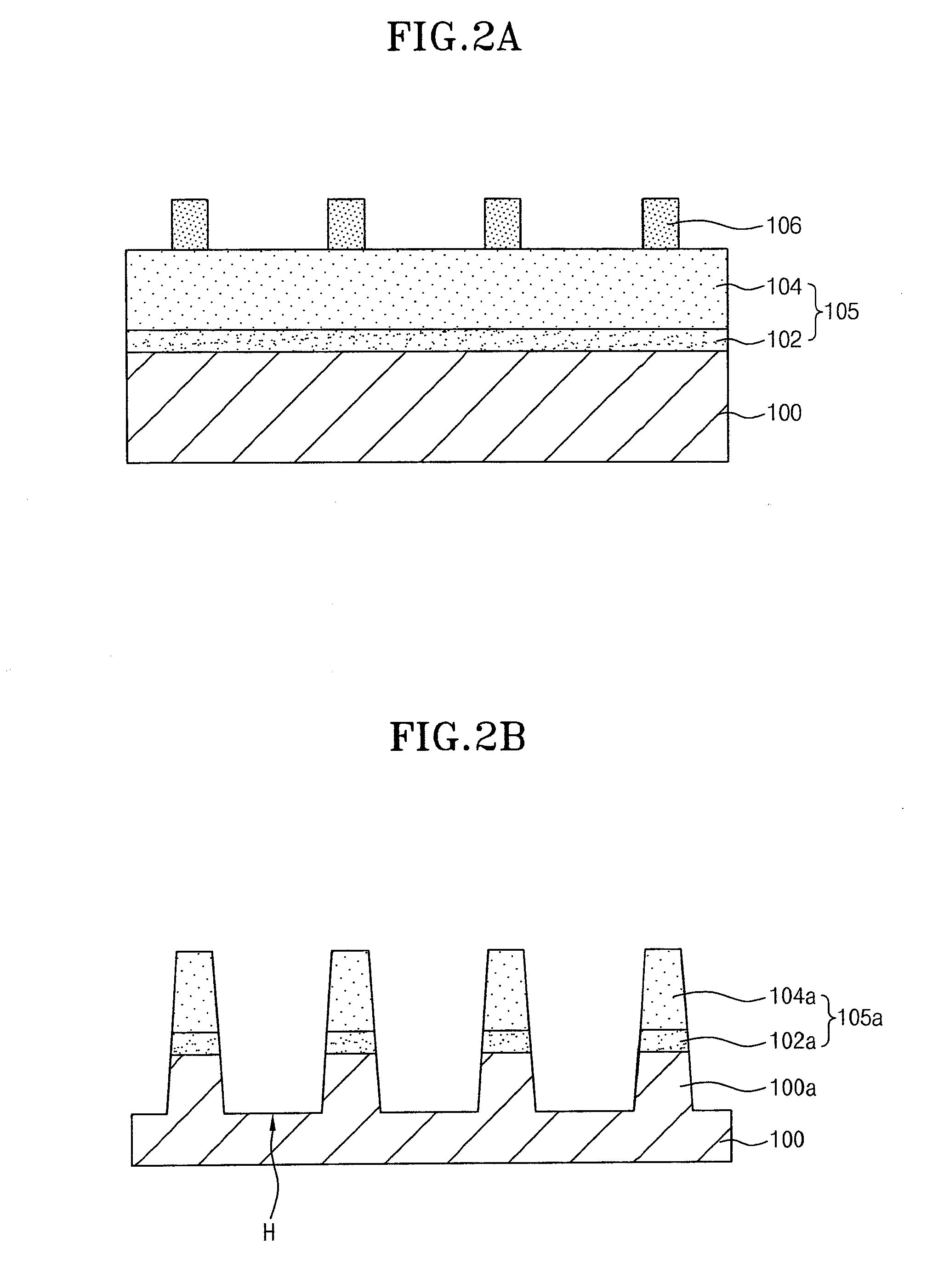
[0031]In the present invention, after the first active patterns are formed to protrude from a semiconductor substrate, second active patterns connected with the first active patterns and having a width greater than that of the first active patterns, are formed from a selective epitaxial growth layer.

[0032]In the present invention wide active regions can be obtained as a result of the forming of the second active patterns, and current amount can increase as channel width increases and channel resistance decreases. Also, in the present invention, due to the fact that the wide active regions can be obtained, contact resistance can be decreased because the open area margins of storage node contacts and bit line contacts can be increased,. Accordingly, in the present invention, it is possible to realize a semiconductor device which has an improved operation characteristic and an increased manufacturing yield.

[0033]Hereafter, specific embodiments of the present invention will be described...


PUM


Abstract

The disclosed semiconductor device includes a plurality of active patterns including first active patterns which protrude from a semiconductor substrate and have a first width and second active patterns which are connected to upper ends of the respective first active patterns and have a second width greater than the first width. The semiconductor device further includes isolation patterns respectively located between the active patterns to insulate the active patterns from one another.

Description

CROSS-REFERENCE TO RELATED APPLICATIONS[0001]The present application claims priority to Korean patent application number 10-2007-0110610 filed on Oct. 31, 2007, which is incorporated herein by reference in its entirety.BACKGROUND OF THE INVENTION[0002]The present invention relates to a semiconductor device and a method for manufacturing the same, and more particularly, to a semiconductor device and a method for manufacturing the same which can improve operation characteristics and increase a manufacturing yield.[0003]As the semiconductor device abruptly shrinks, the channel length and the channel width of the transistor decrease, and the doping concentration of a junction region and junction leakage current increase. In an effort to increase the channel length and the channel width of the transistor, research has actively been conducted to realize a semiconductor device having a three-dimensional channel structure.[0004]For example, a fin transistor has been disclosed in the related...

Claims


Application Information

Patent Timeline
IPC IPC(8): H01L29/06H01L21/762
CPCH01L29/66795H01L21/76232H01L21/18H01L21/762
Inventor CHOI, SHIN GYU
Owner SK HYNIX INC
Why Eureka
Try Eureka