Electrostatic discharge protection apparatus and method therefor
- Summary
- Abstract
- Description
- Claims
- Application Information
AI Technical Summary
Problems solved by technology
Method used
Image
Examples
Embodiment Construction
[0009]Throughout the following description identical reference numerals will be used to identify like parts.
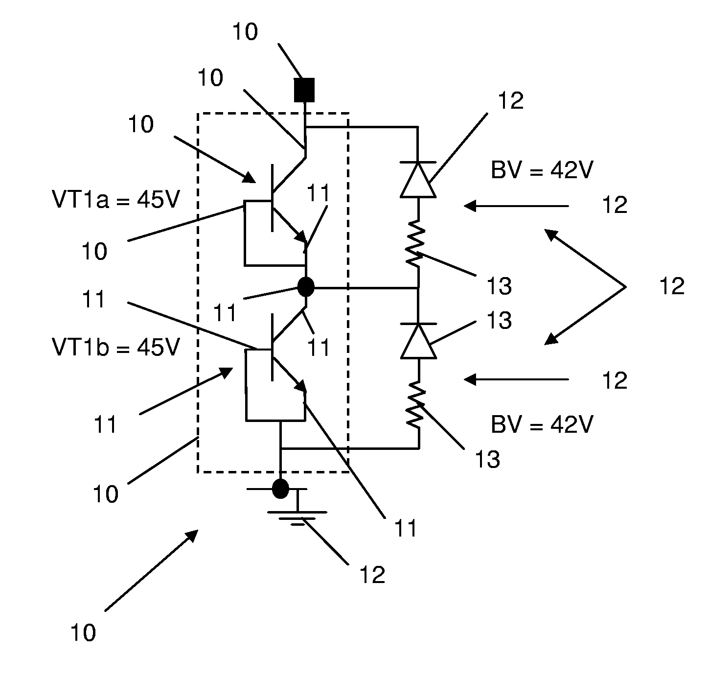
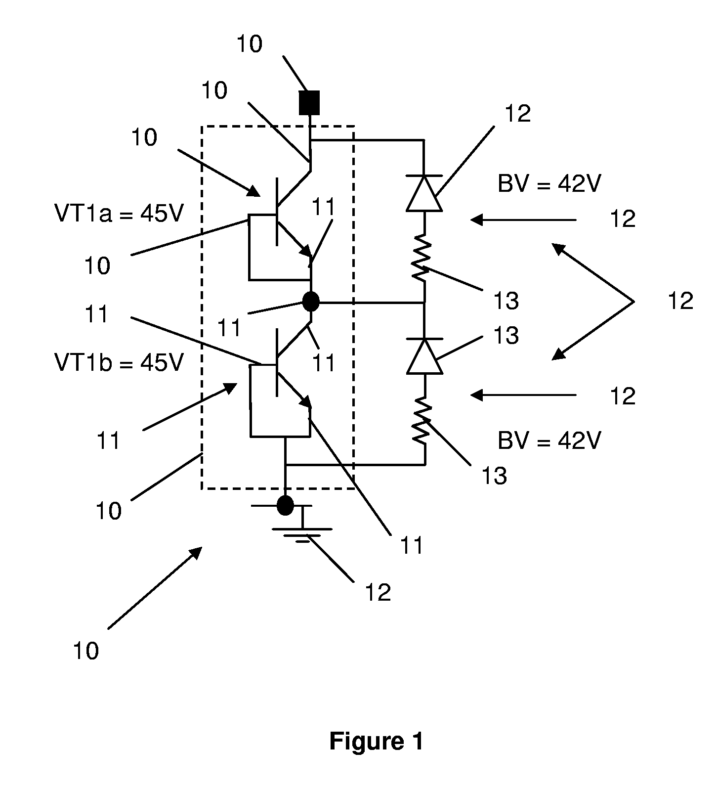
[0010]Referring to FIG. 1, an Electrostatic Discharge (ESD) protection apparatus 100 comprises a stack 101 having a first NPN bipolar transistor 102 having a first collector terminal 104 thereof coupled to a pad 106 of an integrated circuit (not shown) in order to protect circuitry or a device (also not shown) coupled to the pad 106. The first NPN transistor 102 is self-biased and so has a first base terminal 108 coupled to a first emitter terminal 110 thereof.
[0011]The first base and first emitter terminals 108, 110 of the first NPN transistor 102 are coupled to a second collector terminal 112 of a second NPN bipolar transistor 114. As a result of the coupling of the first NPN transistor 102 to the second NPN transistor 114, a notional topological node 115 exists between the first and second NPN transistors 102, 114.
[0012]The second NPN transistor 114 is also self-biased and ...
PUM
 Abstract
Description
Claims
Application Information


