Electro-static discharge protection circuit and method for fabricating the same

Active Publication Date: 2006-07-06
KEY FOUNDRY CO LTD
View PDF4 Cites 72 Cited by
  • Summary
  • Abstract
  • Description
  • Claims
  • Application Information

AI Technical Summary

Benefits of technology

[0026] It is another object of the present invention to provide an ESD protection circuit capable of settling a limitation which each finger

Problems solved by technology

Fourthly, the ESD protection circuit is not operated irregularly by a latch-up.
However, in case that the distance S is excessively decreased, a leakage current may be increased when a voltage lower than the avalanche breakdown voltage is coupled.
However, the current flowed into the N-EDSCR device is increased, a parasitic PNP BJT is operated.
However, although the current flowed into the N-EDSC

Method used


Image

  • Electro-static discharge protection circuit and method for fabricating the same
  • Electro-static discharge protection circuit and method for fabricating the same
  • Electro-static discharge protection circuit and method for fabricating the same

Examples


first embodiment

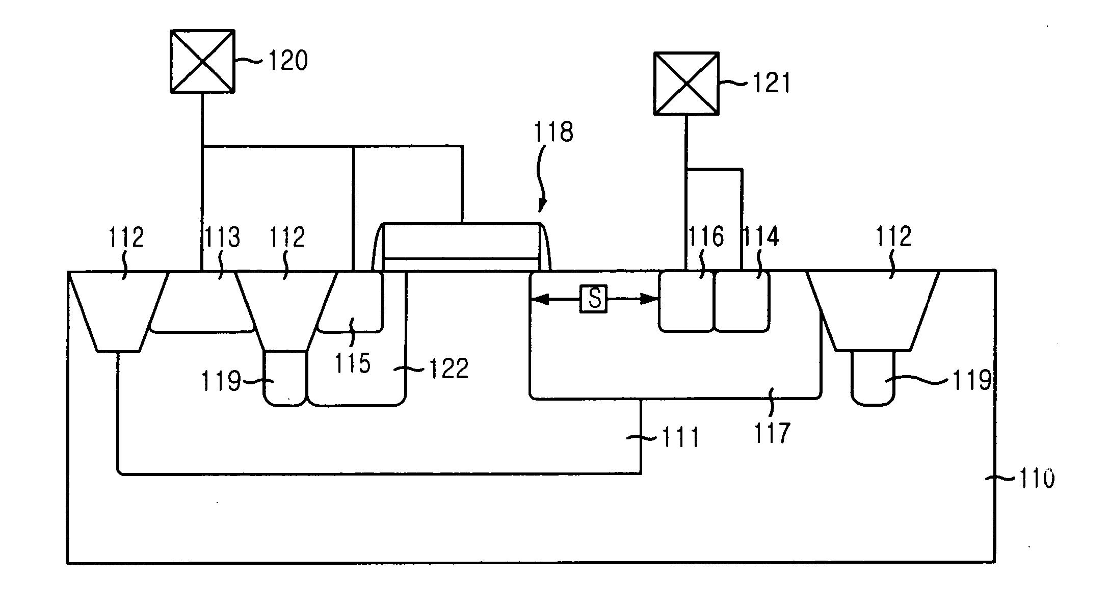
[0045]FIG. 5 is a cross-sectional view illustrating an electro-static discharge (ESD) protection circuit in accordance with the present invention.

[0046] As shown in FIG. 5, for the ESD protection circuit in accordance with the first embodiment of the present invention, a P-type well region 111 is reduced compared to an N-type extended drain silicon controlled rectifier (N-EDSCR) structure. Accordingly, a portion or the whole of a N−-type drift region 117, an N+-type diffusion region 116 for an anode electrode and a P+-type diffusion region 114 for an anode electrode existing inside the N-type drift region 117 are exposed to a substrate 110.

[0047] The P-type well region 111 includes a P+-type diffusion region 113 for a cathode electrode and an N+-type diffusion region 115 for a cathode electrode. Furthermore, the P-type well region 111 may include a predetermined portion of the N−-type drift region 117 to be overlapped with the predetermined portion of the N−-type drift region 117. ...

second embodiment

[0092]FIG. 14 is a cross-sectional view illustrating a modified embodiment of the N-EDSCR_CPS_Bi device shown in FIG. 12. As described above, although the structure in which the partial P-type well structure and the counter pocket source region 722 are formed is exemplified in accordance with the present invention, the N-EDSCR_CPS_Bi device can be embodied with only the counter pocket source region 722 without the partial P-type well structure as shown in FIG. 14.

[0093]FIG. 15 is a cross-sectional view illustrating a multi-finger structure embodied by using the N-EDSCR_CPS_Bi device shown in FIG. 14.

[0094] As shown in FIG. 15, each finger structure shares one P-type well 811 unlike the multi-finger structure shown in FIG. 13. That is, the P-type well 811 includes a plurality of P+-type diffusion layer 813 for a cathode electrode, a plurality of N+-type diffusion layer 815 for a cathode electrode, a plurality of N−-type drift regions 817, a plurality of N+-type diffusion layer 816 f...


PUM


Abstract

An ESD protection circuit using an N-type extended drain silicon controlled rectifier (N-EDSCR) and a method for fabricating the same are provided. An electro-static discharge (ESD) protection circuit includes a substrate, a well formed in the substrate, a drift region having a predetermined portion overlapped with the well, a plurality of first diffusion layers respectively formed in the well and the drift region, a plurality of second diffusion layers respectively formed in the well and the drift region, wherein corresponding first and second diffusion layers in the well are formed separately from each other and those in the drift region are formed adjacent to each other, a source region formed in a manner of surrounding a second conductive type diffusion layer inside the well, and a gate electrode formed on the well between the source and the drift region.

Description

FIELD OF THE INVENTION [0001] The present invention relates to an electro-static discharge (ESD) protection circuit and a method for fabricating the same; and more particularly, to an ESD protection circuit using an N-type extended drain silicon controlled rectifier (N-EDSCR) and a method for fabricating the same. DESCRIPTION OF RELATED ARTS [0002] It is necessary to have a tolerance with respect to a serge voltage and a serge current caused by an electro-static discharge (ESD) given on an input / output pad of a semiconductor chip. So far as mentioned above, an ESD protection circuit is typically connected to the input / output pad of the semiconductor chip. [0003] Typically, the ESD protection circuit should be satisfied with the following basic operation conditions. The basic operation conditions of the ESD protection circuit will be explained in detail with reference to FIG. 1. [0004] First, in case that a normal operation voltage (Vop) is coupled to a semiconductor chip, i.e., a mi...

Claims


Application Information

Patent Timeline
IPC IPC(8): H01L23/62
CPCH01L27/0262H01L29/7436H01L29/749H01L29/87H01L27/04
Inventor KIM, KIL-HO
Owner KEY FOUNDRY CO LTD
Why Eureka
Try Eureka