

Electrostatic discharge protection structures for high speed technologies with mixed and ultra-low voltage supplies
a protection structure and high-speed technology, applied in the direction of overvoltage protection resistors, emergency protective arrangements for limiting excess voltage/current, etc., can solve the problems of gate oxides that are subject to damage at turn-on and high current clamping voltages greater than approximately 4-6 volts
- Summary
- Abstract
- Description
- Claims
- Application Information
AI Technical Summary
Problems solved by technology
Method used
Image

Examples
first embodiment
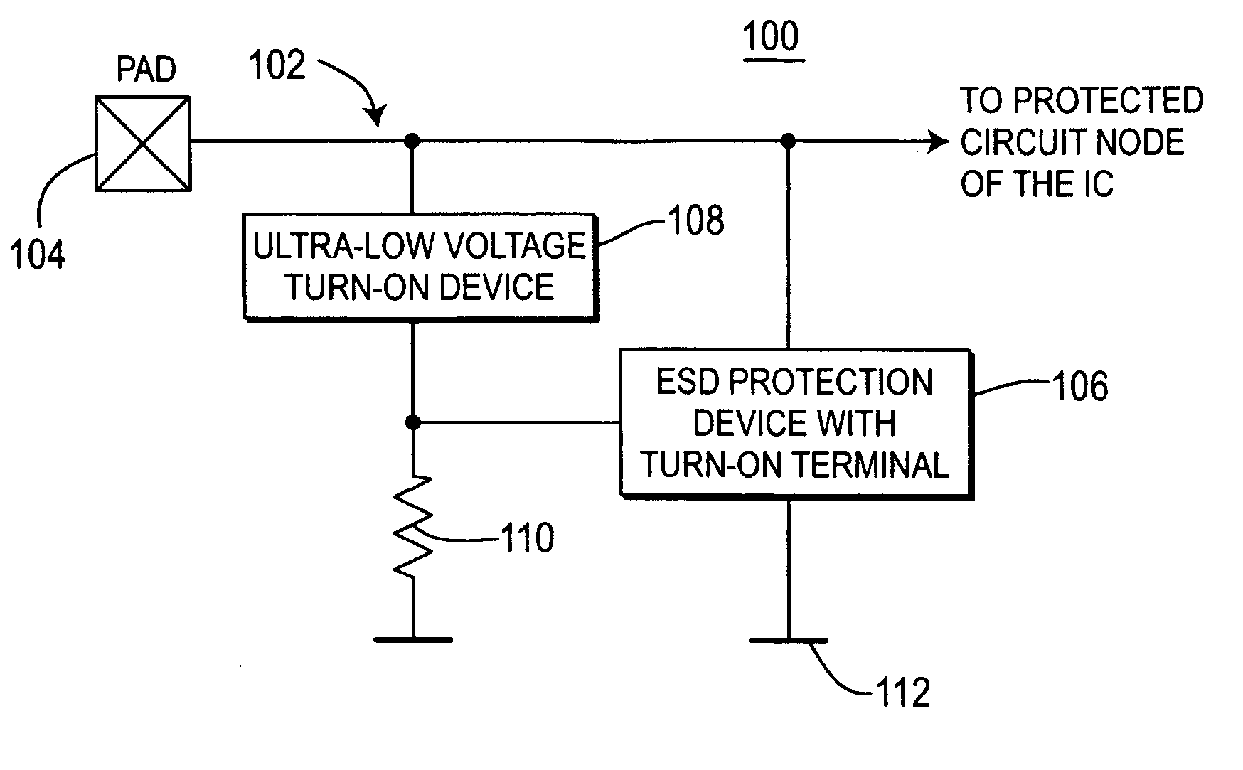
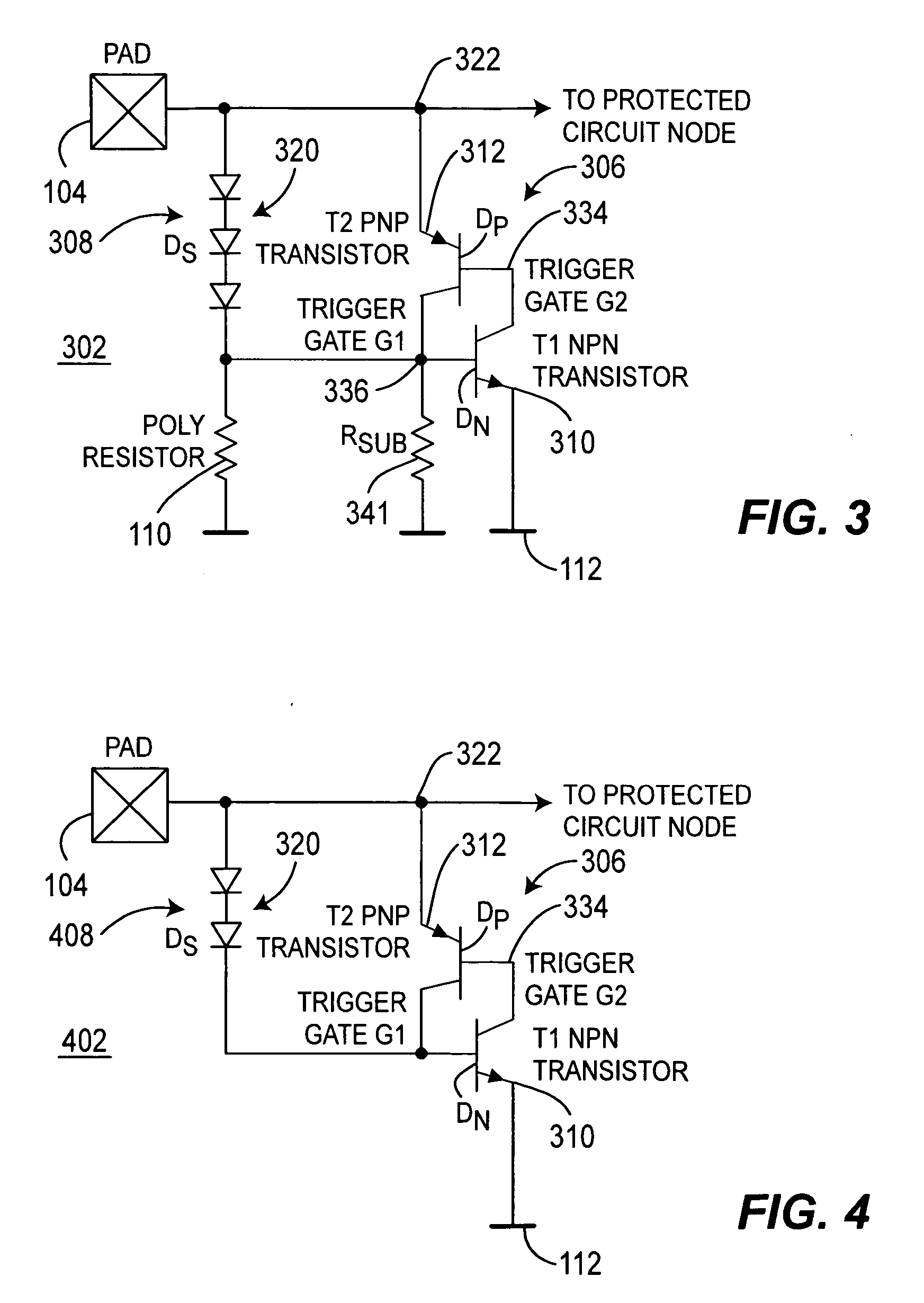
[0027]FIG. 3 depicts a schematic diagram of an ESD protection device 302. In particular, FIG. 3 depicts a schematic diagram of a diode turn-on SCR (DTSCR) protection device 302 of the present invention. The DTSCR 302 comprises a diode turn-on (“triggering”) device 308 and a SCR 306, which together serve as a protection device 302 for the circuitry on an integrated circuit (IC) 100. The DTSCR protection device 302 protects the IC circuitry from electrostatic discharges (ESD) that may occur at the pad 104, which is coupled to the IC circuitry. When turned on, the SCR 306 functions as a shunt to redirect any ESD currents from the pad 104 to ground. The diode turn-on trigger device 308 turns on, that is “triggers”, the SCR 306 to avoid an over-voltage ESD condition.
[0028] Referring to the schematic diagram of FIG. 3, the SCR protection device 306 is illustratively represented as an NPN transistor T1310 and a PNP transistor T2312, as is well known in the art. The emitter of the PNP trans...
second embodiment
[0035]FIG. 4 depicts a schematic diagram of the ESD protection device 402 of the present invention. In particular, FIG. 4 depicts a schematic diagram of the DTSCR protection device 402. The configuration of the diode turn-on SCR protection device 402 is configured the same as the DTSCR protection device 302 of FIG. 3, except that the SCR is fabricated in a process with an isolated P-well, and the substrate resistor 341 is not coupled between the first node 336 and ground 112. Furthermore, the poly shunt resistor 110 is not coupled between the first node 336 and ground 112. Moreover, one less diode is required in the diode chain 320, than used in the diode chain 320 of FIG. 3. In FIG. 4, the diode chain 320 of the diode turn-on device 408 comprises two diodes Ds.
[0036] The SCR 306 of the DTSCR protection device 402 triggers at a lower diode turn-on voltage than the first embodiment 302 of FIG. 3. Specifically, an ESD event occurring at the pad 104, which is positive with respect to g...
fourth embodiment
[0038]FIG. 6 depicts a schematic diagram of the ESD protection device 602 of the present invention. In particular, FIG. 6 depicts a schematic diagram of the DTSCR protection device 602, where the DTSCR 602 is the same as the DTSCR protection device 302 of FIG. 3, except that the trigger gate G2 at the second node 334 is coupled to a positive supply voltage VDD 604. A large N+ doped region is provided in the N-well of the SCR 306, adjacent to the P+ doped region formed in the N-well, which serves as the anode 322 of the SCR 306.
[0039] The P+ region in the N-well serves dual purposes. First, the P+ to N-well junction forms the emitter-base diode Dp of the PNP transistor T2312. Second, the P+ region and adjacent high doped N+ region also form the large emitter-base diode Dp in the PNP transistor T2312, which is connected to the positive supply voltage VDD 604. The coupling of the diode Dp to VDD 604 is often needed to cover other ESD stress types and polarities. Incorporating the diode...
PUM
 Abstract
Description
Claims
Application Information