Eureka AIR delivers breakthrough ideas for toughest innovation challenges, trusted by R&D personnel around the world.

Touch panel and display device using the same

Active Publication Date: 2009-06-18
HON HAI PRECISION IND CO LTD +1
View PDF99 Cites 11 Cited by
  • Summary
  • Abstract
  • Description
  • Claims
  • Application Information

AI Technical Summary

Benefits of technology

[0008]In operation, an upper surface of the touch panel is pressed / touched with a touch tool, such as a user's finger or an electrical pen / stylus. Visual observation of a screen on the liquid crystal display device provided on a backside of the touch panel is possible. In use, because of an electrical field of the user, a coupling capacitance forms between the user and the transparent conductive layer. For high frequency electrical current, the coupled capacitance is a conductor, and thus the touch tool takes away a little current from the touch point. Current flowing through the four electrodes cooperatively replaces the current lost at the touch point. The quantity of current supplied by the four electrodes is directly proportional to the distances from the touch point to the electrodes. A touch panel controller is used to calculate the proportion of the four supplied currents, thereby detecting coordinates of the touch point on the touch panel.

Problems solved by technology

The optically transparent conductive layer (e.g., ITO layer) is generally formed by means of ion-beam sputtering, and this method is relatively complicated.
Furthermore, the ITO layer has generally poor mechanical durability, low chemical endurance, and uneven resistance over an entire area of the touch panel.
Additionally, the ITO layer has relatively low transparency.
All the above-mentioned problems of the ITO layer tend to yield a touch panel with somewhat low sensitivity, accuracy, and brightness.

Method used


Image

  • Touch panel and display device using the same
  • Touch panel and display device using the same
  • Touch panel and display device using the same

Examples


Embodiment Construction

[0020]Reference will now be made to the drawings to describe, in detail, embodiments of the present touch panel and display device using the same.

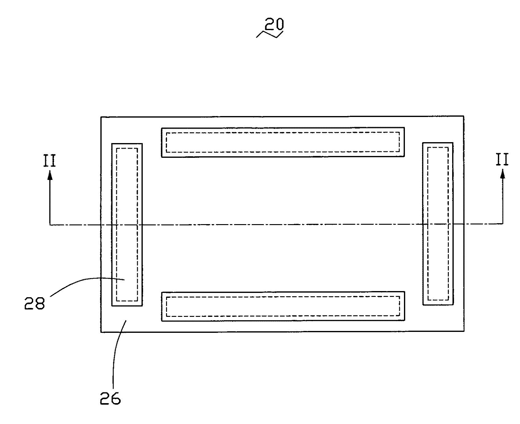
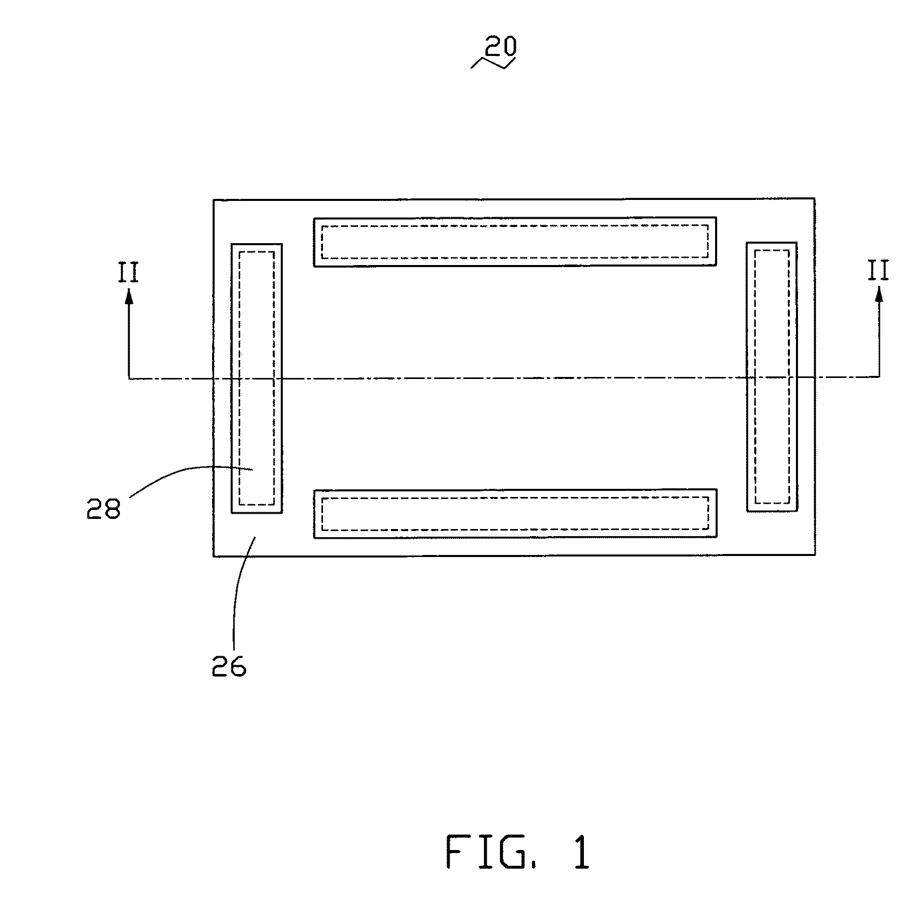
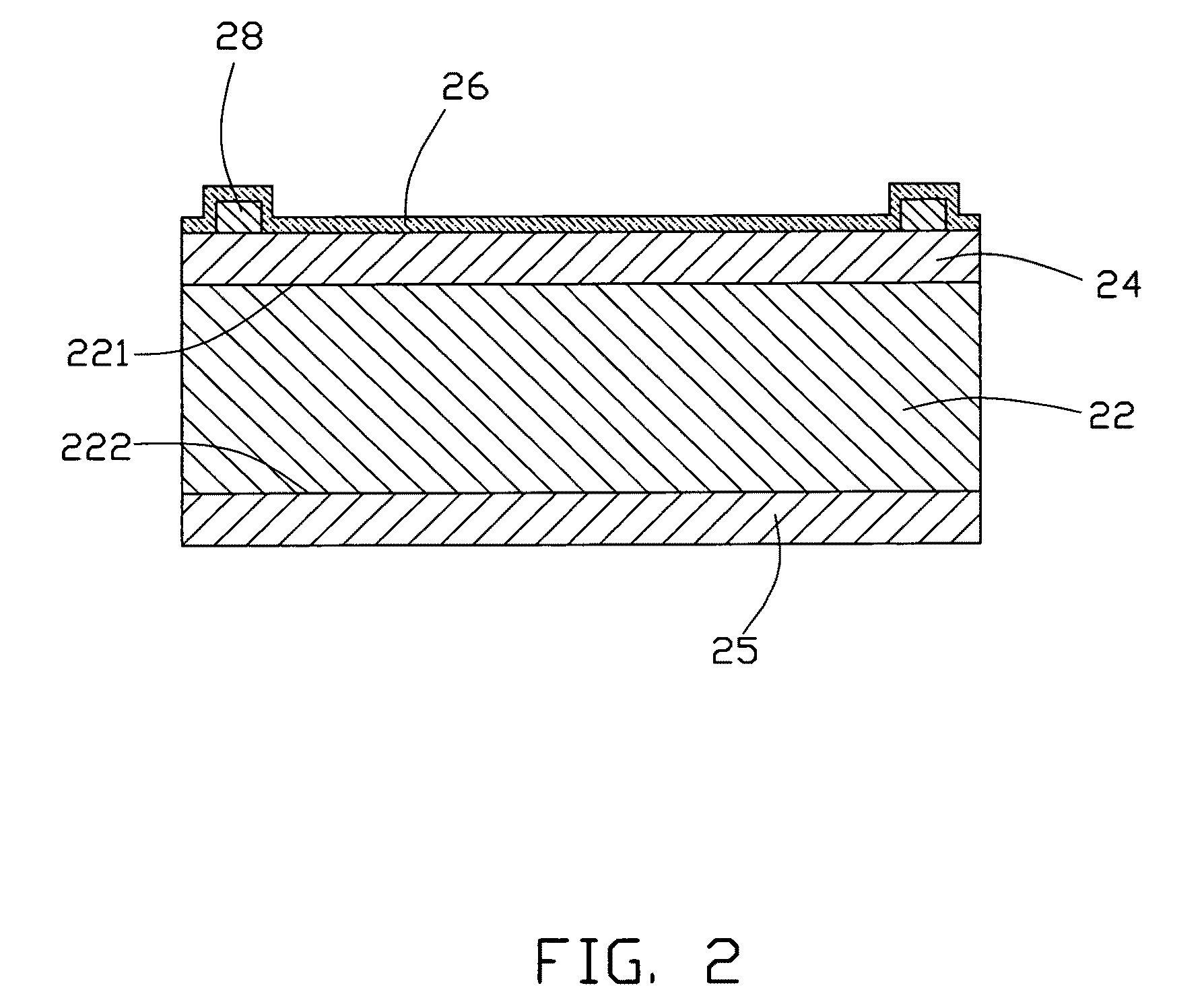
[0021]Referring to FIG. 1 and FIG. 2, a touch panel 20 includes a substrate 22, a transparent conductive layer 24, a transparent protective layer 26, and at least two electrodes 28. The substrate 22 has a first surface 221 and a second surface 222 at opposite sides thereof respectively. The transparent conductive layer 24 is located on the first surface 221. The electrodes 28 are electrically connected with the transparent conductive layer 24 for forming an equipotential surface on the transparent conductive layer 24. The transparent protective layer 26 covers the electrodes 28 and the exposed surface of the transparent conductive layer 24 that faces away from the substrate 22.

[0022]The substrate 22 has a planar structure or a curved structure. The material of the substrate 22 is selected from the group consisting of glass, quartz, diamond...


PUM


Abstract

A touch panel includes a substrate, a transparent conductive layer, and at least two electrodes. The transparent conductive layer is formed on a surface of the substrate. The transparent conductive layer includes a carbon nanotube layer, and the carbon nanotube layer includes a plurality of carbon nanotubes arranged along a same direction. The electrodes are electrically connected with the transparent conductive layer. Further, a display device using the touch panel is also included.

Description

RELATED APPLICATIONS[0001]This application is related to commonly-assigned applications entitled, “TOUCH PANEL”, filed ______ (Atty. Docket No. US17449); “TOUCH PANEL”, filed ______ (Atty. Docket No. US17448); “TOUCH PANEL AND DISPLAY DEVICE USING THE SAME”, filed ______ (Atty. Docket No. US17861); “TOUCH PANEL AND DISPLAY DEVICE USING THE SAME”, filed ______ (Atty. Docket No. US17818); “TOUCH PANEL AND DISPLAY DEVICE USING THE SAME”, filed ______ (Atty. Docket No. US17820); “TOUCH PANEL AND DISPLAY DEVICE USING THE SAME”, filed ______ (Atty. Docket No. US17862); “TOUCH PANEL AND DISPLAY DEVICE USING THE SAME”, filed ______ (Atty. Docket No. US17863); “TOUCH PANEL AND DISPLAY DEVICE USING THE SAME”, filed ______ (Atty. Docket No. US18263); “TOUCHABLE CONTROL DEVICE”, filed ______ (Atty. Docket No. US18262); “TOUCH PANEL AND DISPLAY DEVICE USING THE SAME”, filed ______ (Atty. Docket No. US17889); “TOUCH PANEL AND DISPLAY DEVICE USING THE SAME”, filed ______ (Atty. Docket No. US17884)...

Claims


Application Information

Patent Timeline
IPC IPC(8): G06F3/041
CPCG06F3/041B82Y30/00G06F3/0444
Inventor JIANG, KAI-LILIU, LIANGFAN, SHOU-SHAN
Owner HON HAI PRECISION IND CO LTD
Why Eureka
Eureka Blog
Learn More