Memory cell that employs a selectively fabricated carbon nano-tube reversible resistance-switching element formed over a bottom conductor and methods of forming the same

a technology of reversible resistance and switching element, which is applied in the field of nonvolatile memories, can solve the problems of technical challenges in the manufacture of memory devices from rewriteable resistivity-switching materials

Active Publication Date: 2009-07-02
SANDISK TECH LLC
View PDF40 Cites 120 Cited by
  • Summary
  • Abstract
  • Description
  • Claims
  • Application Information

AI Technical Summary

Benefits of technology

[0008]In a second aspect of the invention, a method of fabricating a memory cell is provided that includes (1) fabricating a first conductor above a substrate; (2) fabricating a reversible resistance-switching element above the first conductor by selectively fabricating carbon nano-tube (CNT) material above the first conductor; (3) fabricating a vertical polycrystalline diode above the reversible resistance-switching element; and (4) fabricating a second conductor above the vertical polycrystalline diode.
[0009]In a third aspect of the invention, a memory cell is provided that includes (1) a first conductor; (2) a reversible resistance-switching element including carbon nano-tube (CNT) material selectively fabricated above the first conductor; (3) a diode formed above the reversible resistance-switching element; and (4) a second conductor formed above the diode.
[0010]In a fourth aspect of the invention, a plurality of nonvolatile memory cells are provided that includes (1) a first plurality of substantially parallel, substantially coplanar conductors extending in a first direction; (2) a plurality of diodes; (3) a plurality of reversible resistance-switching el...

Problems solved by technology

However, fabricating memory devices from rewriteable resistivity-switching materials is technically challenging...

Method used


Image

  • Memory cell that employs a selectively fabricated carbon nano-tube reversible resistance-switching element formed over a bottom conductor and methods of forming the same
  • Memory cell that employs a selectively fabricated carbon nano-tube reversible resistance-switching element formed over a bottom conductor and methods of forming the same
  • Memory cell that employs a selectively fabricated carbon nano-tube reversible resistance-switching element formed over a bottom conductor and methods of forming the same

Examples


first exemplary embodiment

of a Memory Cell

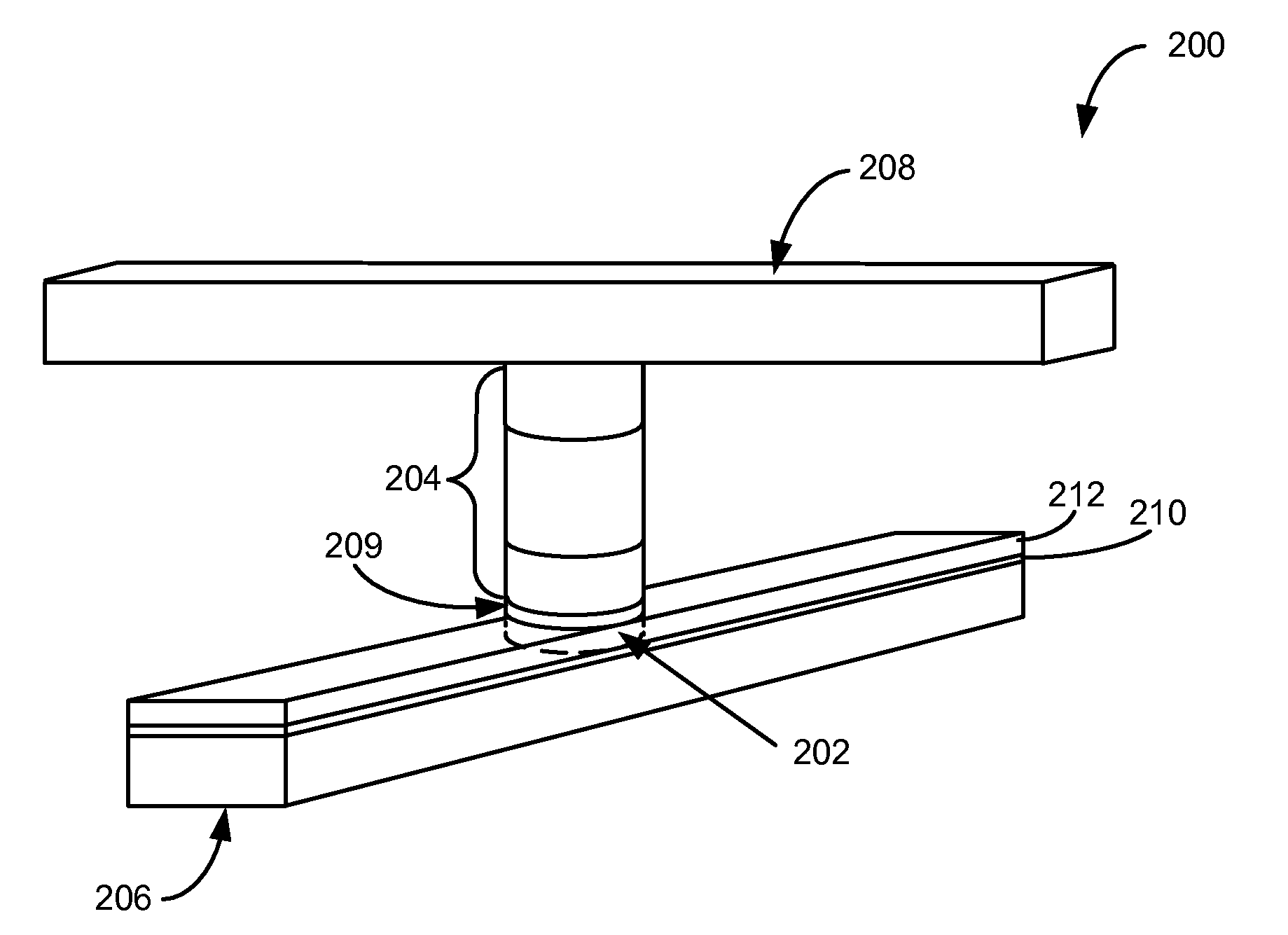
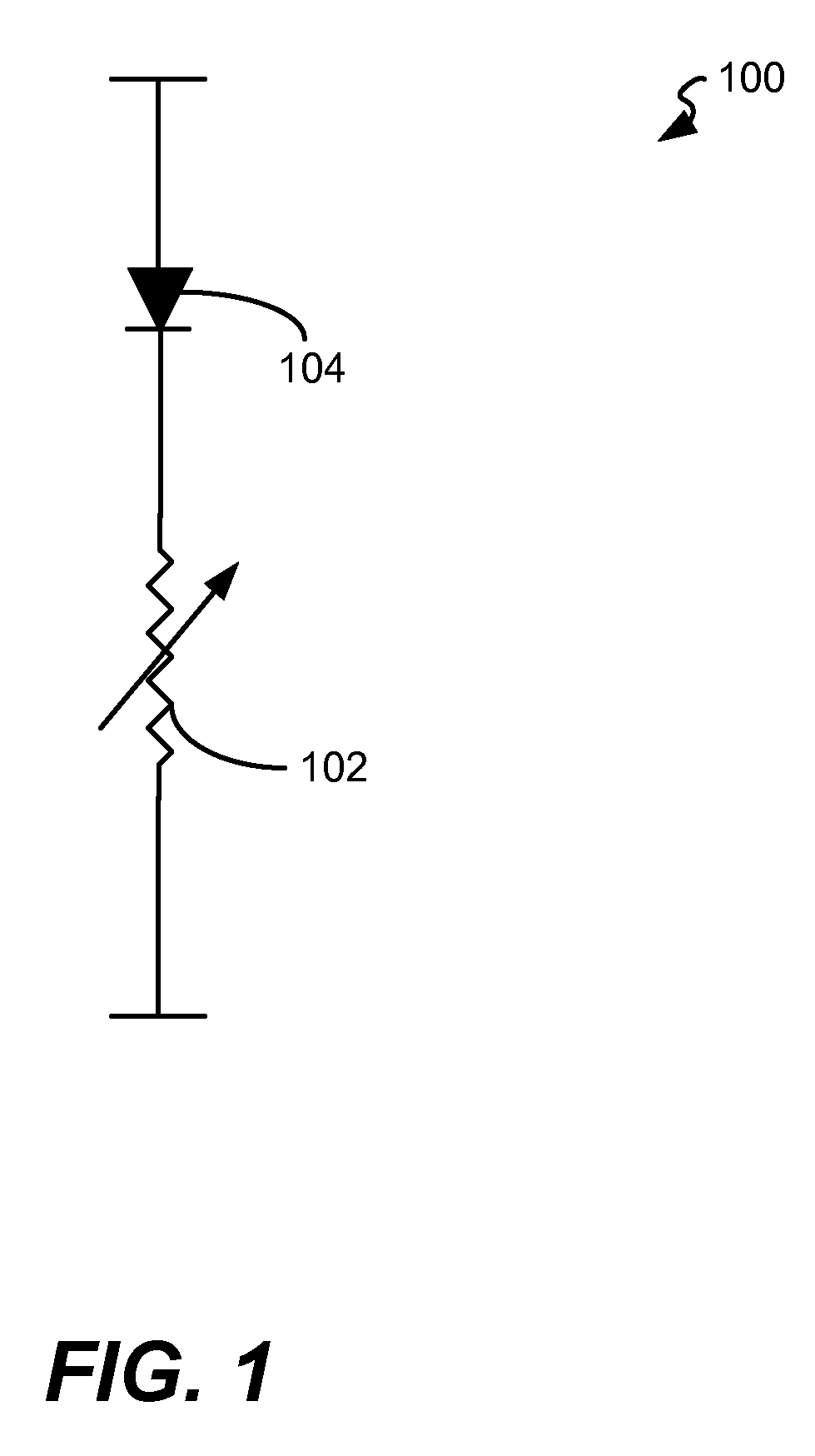
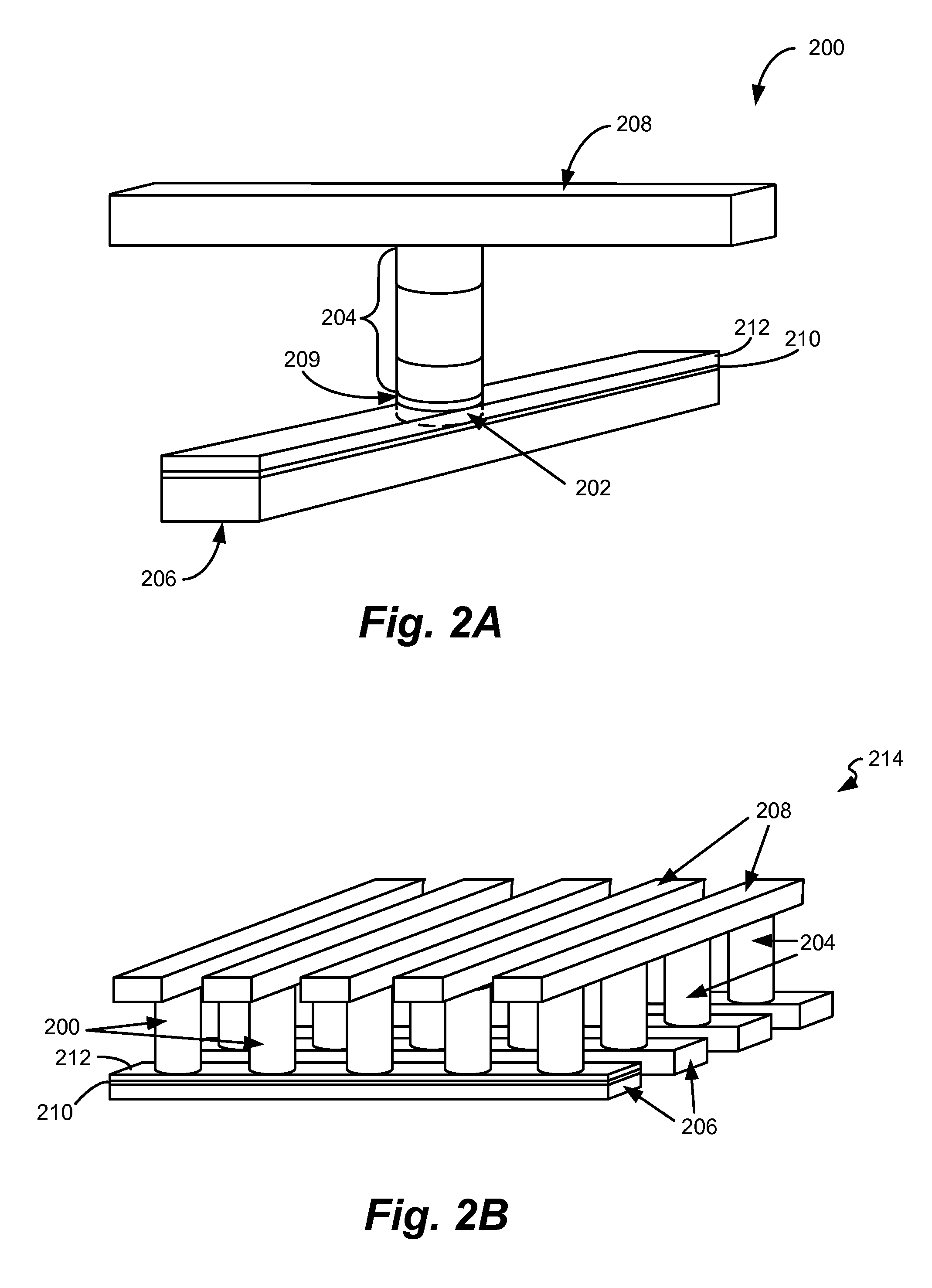
[0033]FIG. 2A is a simplified perspective view of a first embodiment of a memory cell 200 provided in accordance with the present invention. With reference to FIG. 2A, the memory cell 200 includes a reversible resistance-switching element 202 (shown in phantom) coupled in series with a diode 204 between a first conductor 206 and a second conductor 208. In some embodiments, a barrier layer 209 such as titanium nitride, tantalum nitride, tungsten nitride, etc., may be provided between the reversible resistance-switching element 202 and the diode 204.

[0034]As will be described further below, the reversible resistance-switching element 202 is selectively formed so as to simplify fabrication of the memory cell 200. In at least one embodiment, the reversible resistance-switching element 202 includes at least a portion of a CNT material formed on a CNT seeding layer such as titanium nitride, tantalum nitride, nickel, cobalt, iron or the like. For example, a titanium or tant...


PUM


Abstract

In some aspects, a method of fabricating a memory cell is provided that includes (1) fabricating a first conductor above a substrate; (2) selectively fabricating a carbon nano-tube (CNT) material above the first conductor; (3) fabricating a diode above the CNT material; and (4) fabricating a second conductor above the diode. Numerous other aspects are provided.

Description

CROSS REFERENCE TO RELATED APPLICATIONS[0001]The present application is related to the following patent applications which are hereby incorporated by reference herein in their entirety for all purposes:[0002]U.S. patent application Ser. No. ______, filed on even date herewith and titled “MEMORY CELL THAT EMPLOYS A SELECTIVELY FABRICATED CARBON NANO-TUBE REVERSIBLE RESISTANCE-SWITCHING ELEMENT AND METHODS OF FORMING THE SAME” (Docket No. MD-348).[0003]U.S. patent application Ser. No. ______, filed on even date herewith and titled “MEMORY CELL WITH PLANARIZED CARBON NANOTUBE LAYER AND METHODS OF FORMING THE SAME” (Docket No. MD-368).FIELD OF THE INVENTION[0004]The present invention relates to non-volatile memories and more particularly to a memory cell that employs a selectively fabricated carbon nano-tube (CNT) reversible resistance-switching element formed over a bottom conductor and methods of forming the same.BACKGROUND OF THE INVENTION[0005]Non-volatile memories formed from rever...

Claims


Application Information

Patent Timeline
IPC IPC(8): H01L51/30
CPCB82Y10/00G11C13/025G11C2213/72H01L27/285H01L45/04H01L51/0048H01L27/2481H01L51/0591H01L51/0595H01L45/1233H01L45/149H01L45/1616H01L27/2409H01L51/0575H10B63/84H10B63/20H10N70/20H10N70/8845H10N70/023H10N70/826H10K19/202H10K85/221H10K10/20H10K10/50H10K10/701Y10S977/762
Inventor SCHRICKER, APRILCLARK, MARKHERNER, BRAD
Owner SANDISK TECH LLC
Why Eureka
Try Eureka