Three-dimensional liquid crystal polymer multilayer circuit board including membrane switch and related methods

Active Publication Date: 2009-07-23
HARRIS CORP
View PDF26 Cites 28 Cited by
  • Summary
  • Abstract
  • Description
  • Claims
  • Application Information

AI Technical Summary

Benefits of technology

[0008]In view of the foregoing background, it is therefore an object of the present invention to provide an electronic device

Problems solved by technology

Even with the advent of the multilayer circuit board, as the mounted circuitry has become even more complex, the size of the circuit board and associated packaging has also increased.
This increase in size may pose installation drawbacks in appl

Method used


Image

  • Three-dimensional liquid crystal polymer multilayer circuit board including membrane switch and related methods
  • Three-dimensional liquid crystal polymer multilayer circuit board including membrane switch and related methods
  • Three-dimensional liquid crystal polymer multilayer circuit board including membrane switch and related methods

Examples


Embodiment Construction

[0024]The present invention will now be described more fully hereinafter with reference to the accompanying drawings, in which preferred embodiments of the invention are shown. This invention may, however, be embodied in many different forms and should not be construed as limited to the embodiments set forth herein. Rather, these embodiments are provided so that this disclosure will be thorough and complete, and will fully convey the scope of the invention to those skilled in the art. Like numbers refer to like elements throughout.

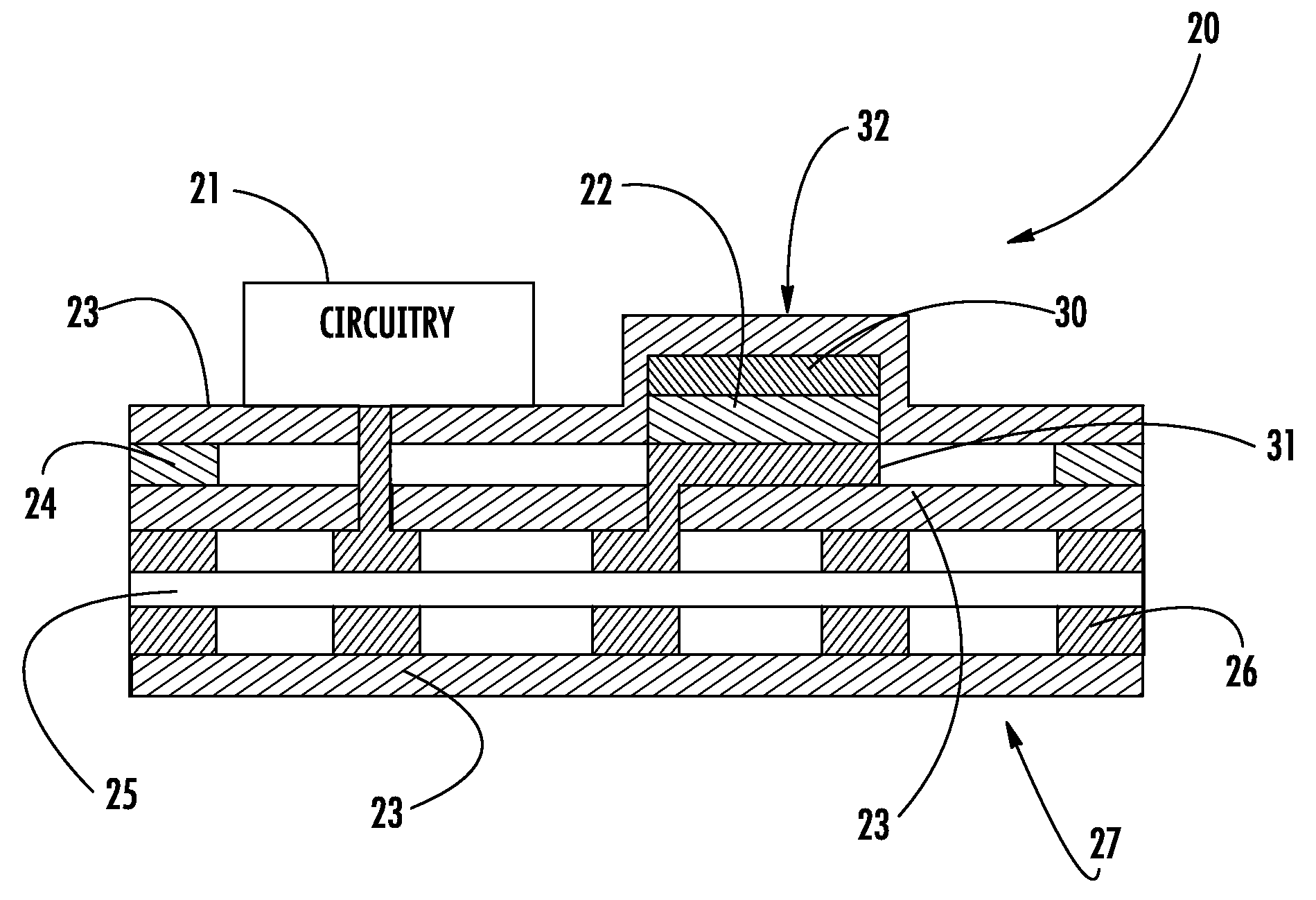
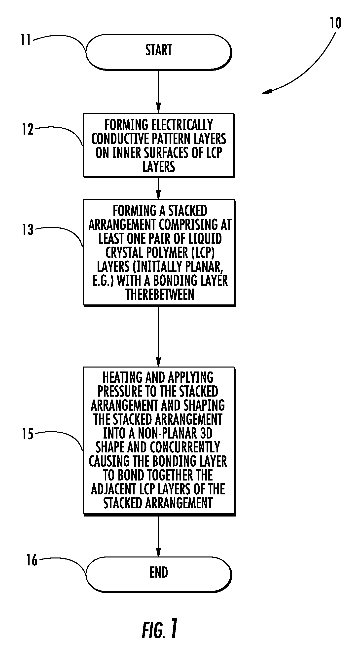
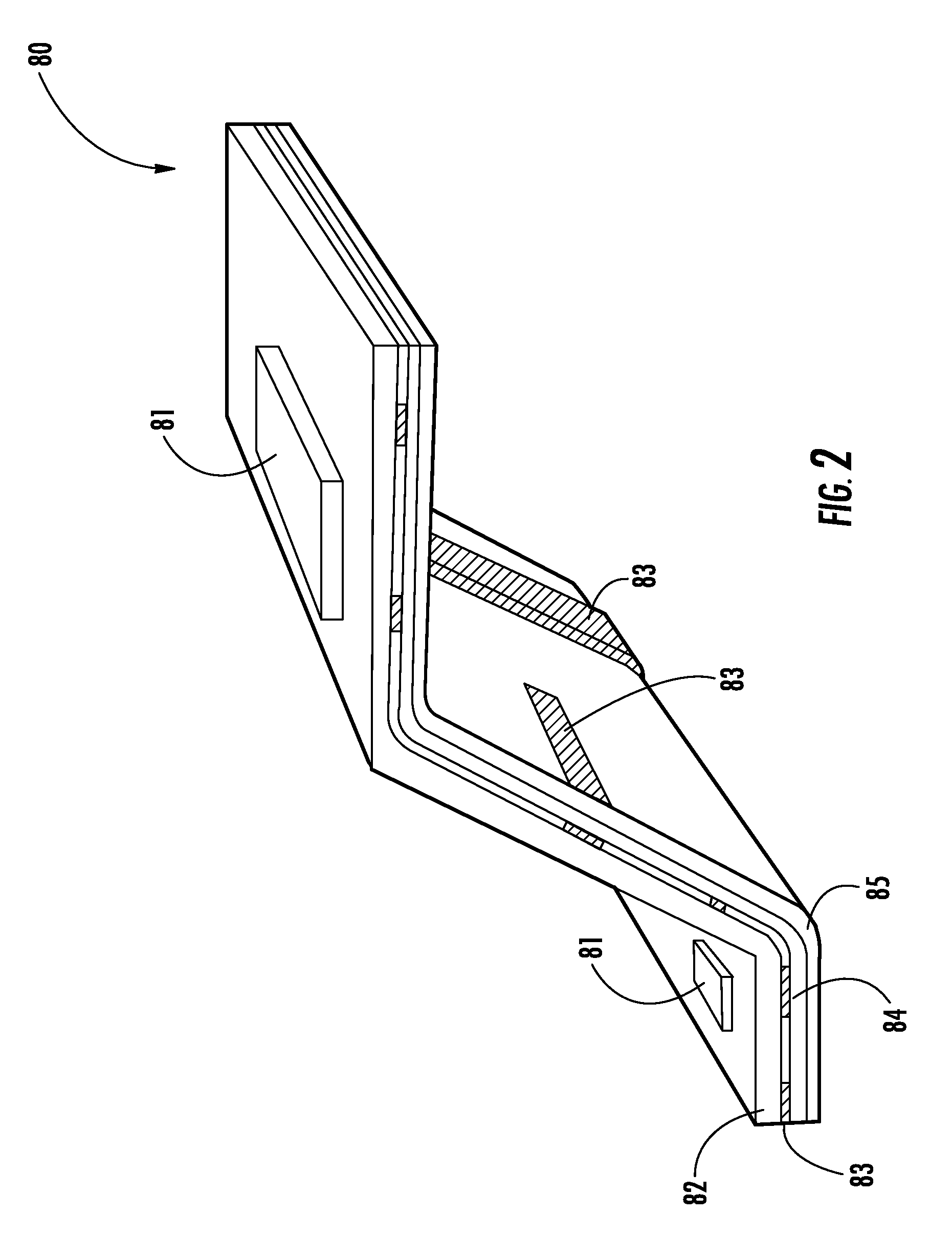
[0025]Referring initially to FIGS. 1-2, a flowchart 10 illustrates a method for making a non-planar three-dimensional (3D) multilayer circuit board 80. From the start (Block 11), the method illustratively includes forming (Block 12) a electrically conductive pattern layer 83 on inner surfaces of liquid crystal polymer (LCP) layers 82, 85, and forming (Block 13) a stacked arrangement, which may be initially planar, the stacked arrangement comprising at leas...


PUM

PropertyMeasurementUnit
Temperatureaaaaaaaaaa
Pressureaaaaaaaaaa
Electrical conductivityaaaaaaaaaa

Abstract

An electronic device includes a multilayer circuit board having a non-planar three-dimensional shape defining a membrane switch recess therein. The multilayer circuit board may include at least one liquid crystal polymer (LCP) layer, and at least one electrically conductive pattern layer thereon defining at least one membrane switch electrode adjacent the membrane switch recess to define a membrane switch. The electronic may further include a compressible dielectric material filling the membrane switch recess. The electronic device may also include at least one spring member within the membrane switch recess.

Description

FIELD OF THE INVENTION[0001]The present invention relates to the field of circuit boards, and, more particularly, to circuit boards including a membrane switch provided therein and related methods.BACKGROUND OF THE INVENTION[0002]An electronic device may include one or more circuit boards. A typical circuit board is a two-dimensional (2D) planar board that mechanically supports electronic components. The electronic components may comprise, for example, resistors, capacitors, switches, batteries, and other more complex integrated circuit components, i.e. microprocessors. The circuit board typically comprises a dielectric material, for example, a plastic material.[0003]The circuit board may include conductive traces on the surface for connecting the electronic components to each other. As electronic circuitry has become more complex, multilayer circuit boards with at least two electrically conductive pattern layers have been developed. Typically, the different conductive trace layers ...

Claims


Application Information

Patent Timeline
IPC IPC(8): H05K1/02H05K3/30
CPCH01H13/704H05K1/0284H05K3/4614Y10T29/4913H05K2201/0141H05K2201/091H05K3/4632Y10T29/49107H05K3/303H05K3/4626H01H11/00
Inventor RENDEK, JR., LOUIS JOSEPHSHACKLETTE, LAWRENCE WAYNEJAYNES, PAUL BRIANMARVIN, PHILIP ANTHONY
Owner HARRIS CORP
Why Eureka
Try Eureka