
Wafer processing method

a processing method and wafer technology, applied in the direction of manufacturing tools, grinding machine components, lapping machines, etc., can solve the problems of reducing productivity, affecting productivity, and affecting the processing time, so as to prevent the occurrence and improve the effect of productivity

Active Publication Date: 2009-07-23
DISCO CORP
View PDF8 Cites 26 Cited by
  • Summary
  • Abstract
  • Description
  • Claims
  • Application Information

AI Technical Summary

Benefits of technology

[0008]Accordingly, it is an object of the present invention to provide a wafer processing method that can suppress the occurrence of a burst chipping at the inner circumferential edge of a reinforcing rib area during rough grinding to prevent the occurrence of a transfer error without impairing productivity.
[0010]According to the wafer producing method of the present invention, the rough grinding using the first grinding stone is divided into the first and second steps. In the first step, the wafer is ground into the concave shape at the first transfer rate with the reinforcing rib area unground. Then, as the primary rough grinding in the second step, the grinding stone is positioned slightly on the inner circumferential side and the wafer is further ground to the concave shape at the second transfer rate faster than the first transfer rate. Since the first transfer rate is suppressed to a rate not to cause a burst chipping, a burst chipping resulting from the second step fast in the processing rate to ensure productivity will occur at the stepped edge portion on the inside of the reinforcing rib area surface. Thus, the flatness of the reinforcing rib area can be ensured to provide an effect of suppressing an error encountered during the transfer of the wafer with the front surface of the reinforcing rib area sucked and held.

Problems solved by technology

However, if the semiconductor wafer is simply thinned, rigidity is reduced, which poses a problem in that the wafer becomes difficult to handle and becomes fragile in the step after the thinning.
In such a case, there is a problem in that not only time required for processing lengthens to lower productivity but also the grinding stone wears out fast to increase consumable tool expenses.
Thus, while the drum wafer is transferred to a subsequent step with the outer circumferential reinforcing rib area sucked and held, leak occurs at the concave portion to disturb normal suction and holding, thereby causing a transfer error.

Method used


Image

  • Wafer processing method
  • Wafer processing method
  • Wafer processing method

Examples


Embodiment Construction

[0019]A description is given of a wafer processing method according to preferred embodiments of the present invention with reference to the drawings. The present invention is not limited to the embodiments and can be modified in various ways without departing from the gist thereof.

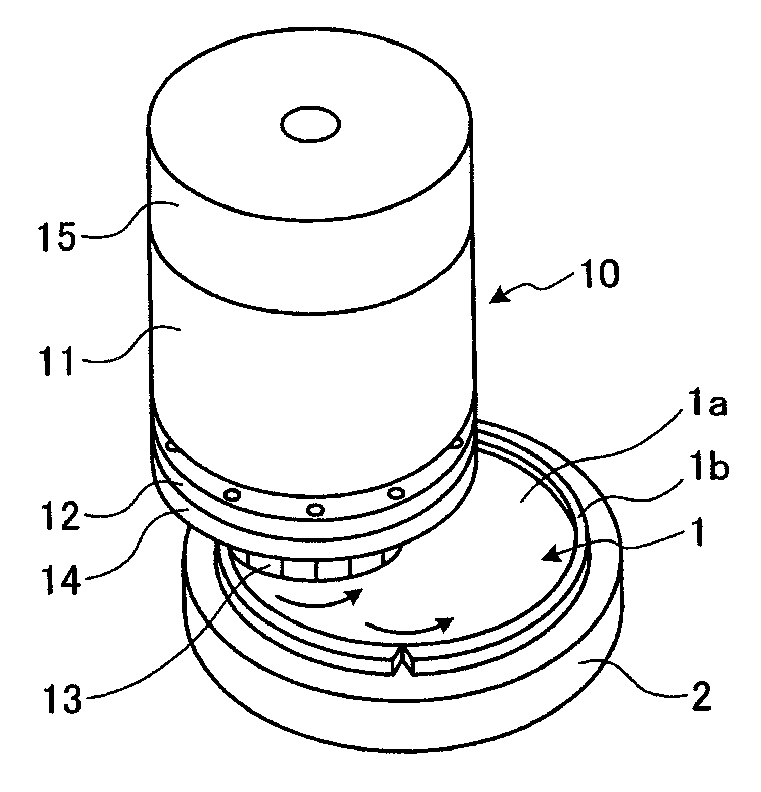
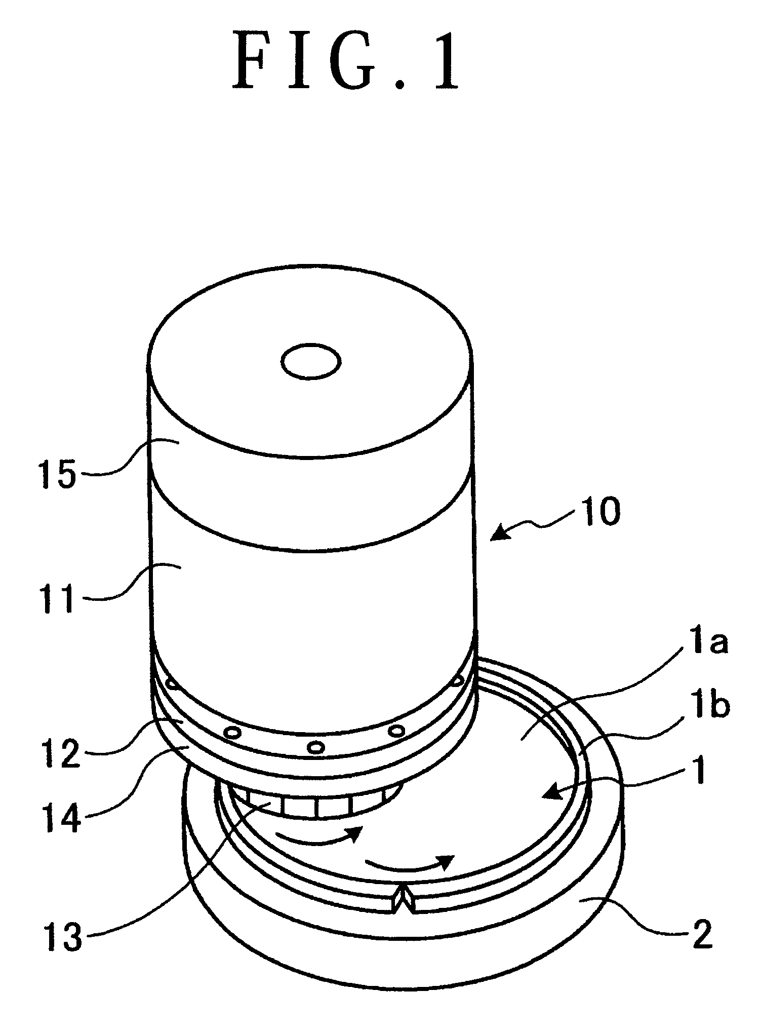
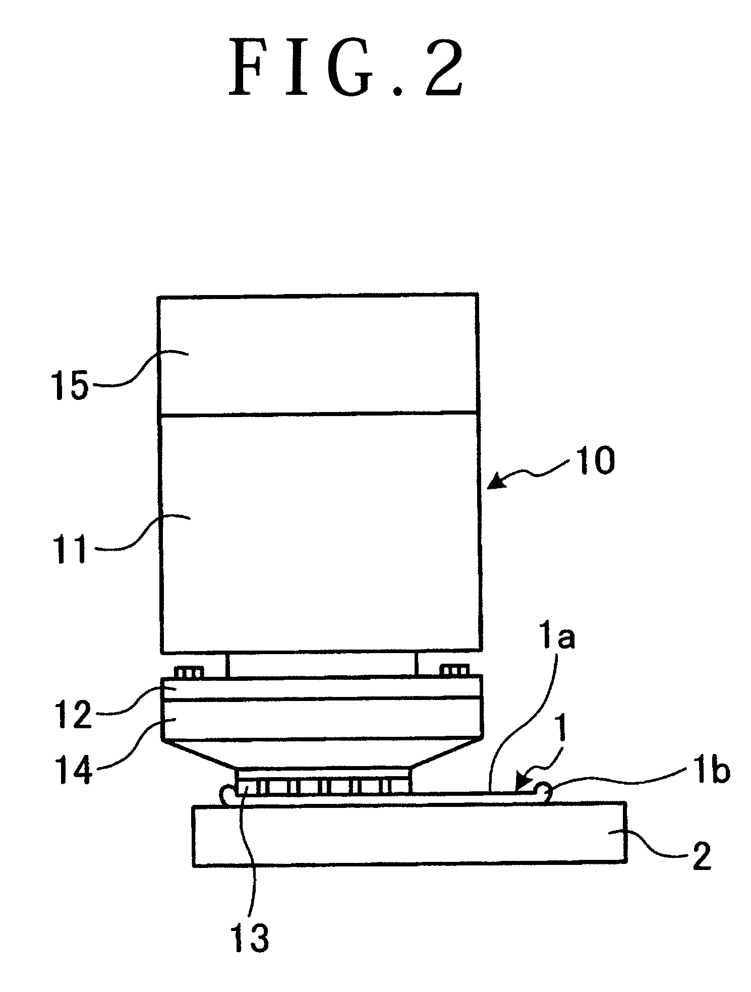
[0020]FIG. 1 is a perspective view illustrating a configurational example of first grinding means and its associated parts used in first and second steps for rough grinding. FIG. 2 is a front view of FIG. 1. FIG. 3 is a perspective view illustrating a configurational example of second grinding means and its associated parts used in a third step for finish grinding. FIG. 4 is a front view of FIG. 3. FIGS. 5A to 5C are schematic step diagrams sequentially illustrating positioning of a grinding stone in the respective steps by way of example. FIG. 6 is an enlarged cross-sectional view of a wafer subjected to processing in the steps by way of example. FIG. 7 is a cross-sectional view of a wafer subjected to tr...


PUM

PropertyMeasurementUnit
sizeaaaaaaaaaa
thicknessaaaaaaaaaa
thicknessaaaaaaaaaa

Abstract

In a wafer processing method, rough grinding using a first grinding stone is divided into first and second steps. In the first step, a wafer is processed into a concave shape at a first transfer rate with a reinforcing rib area slightly left. Thereafter, as primary rough grinding in the second step, the grinding stone is positioned slightly on the inner circumferential side and the wafer is further processed into the concave portion at a second transfer rate faster than the first transfer rate. Since the first transfer rate is suppressed to a rate not to cause a burst chipping, a burst chipping resulting from the second step fast in the processing rate to ensure productivity will occur at the stepped edge portion on the inside of the reinforcing rib area surface. Thus, the flatness of the reinforcing rib area can be ensured.

Description

BACKGROUND OF THE INVENTION[0001]1. Field of the Invention[0002]The present invention relates to a wafer processing method for performing grinding processing while leaving a thick reinforcing rib area at the outer circumferential edge of a wafer.[0003]2. Description of the Related Art[0004]Semiconductor chips used in various electronic devices are generally manufactured by the following method. The front surface of a disk-like semiconductor wafer is sectioned along predetermined dividing lines into lattice-like rectangular areas. Electronic circuits are formed on the front surfaces of the areas. Then, the semiconductor wafer is thinly ground from the rear surface and divided along the predetermined dividing lines. Incidentally, electronic devices have significantly been reduced in size and in thickness in the recent years. Along with this, the semiconductor chips are required to have a smaller thickness. Therefore, the semiconductor wafer is needed to be thinner than ever before. Ho...

Claims


Application Information

Patent Timeline
Patent Type & Authority Applications(United States)
IPC IPC(8): B24B1/00H01L21/304
CPCB24B37/042B24B7/228Y10S438/959
Inventor TAKAHASHI, AKINAGASHIMA, MASAAKI
Owner DISCO CORP
Learn More