
Thin film transistor, contact structure, substrate, display device, and methods for manufacturing the same

a thin film transistor and contact structure technology, applied in the field of thin film transistors and contact structures, can solve the problems of inability to ensure the appropriate ohmic contact, disadvantageous difficulty in providing a high-precision small transistor, and inability to ensure the stability of connection using the minute contact hole, so as to achieve better electrical characteristics and reliability, and improve productivity. the effect of reliability

Active Publication Date: 2014-05-13
SHARP KK
View PDF23 Cites 7 Cited by
  • Summary
  • Abstract
  • Description
  • Claims
  • Application Information

AI Technical Summary

Benefits of technology

The present invention enables the formation of TFTs with better electrical characteristics and reliability without compromising productivity.

Problems solved by technology

In the structure, however, it is necessary to highly precisely form the two contact holes with a predetermined clearance, and therefore, it is disadvantageously difficult to provide a high-precision small transistor.
It is also disadvantageously difficult to ensure a stable connection using the minute contact hole.
Moreover, at a portion where the metal oxide semiconductor and the electrode are joined together, if oxygen contained in the metal oxide semiconductor migrates to the electrode, an oxide is formed on the surface of the electrode and acts as an electrical barrier, so that an appropriate ohmic contact may not be ensured.

Method used


Image

  • Thin film transistor, contact structure, substrate, display device, and methods for manufacturing the same
  • Thin film transistor, contact structure, substrate, display device, and methods for manufacturing the same
  • Thin film transistor, contact structure, substrate, display device, and methods for manufacturing the same

Examples


first embodiment

[0080]

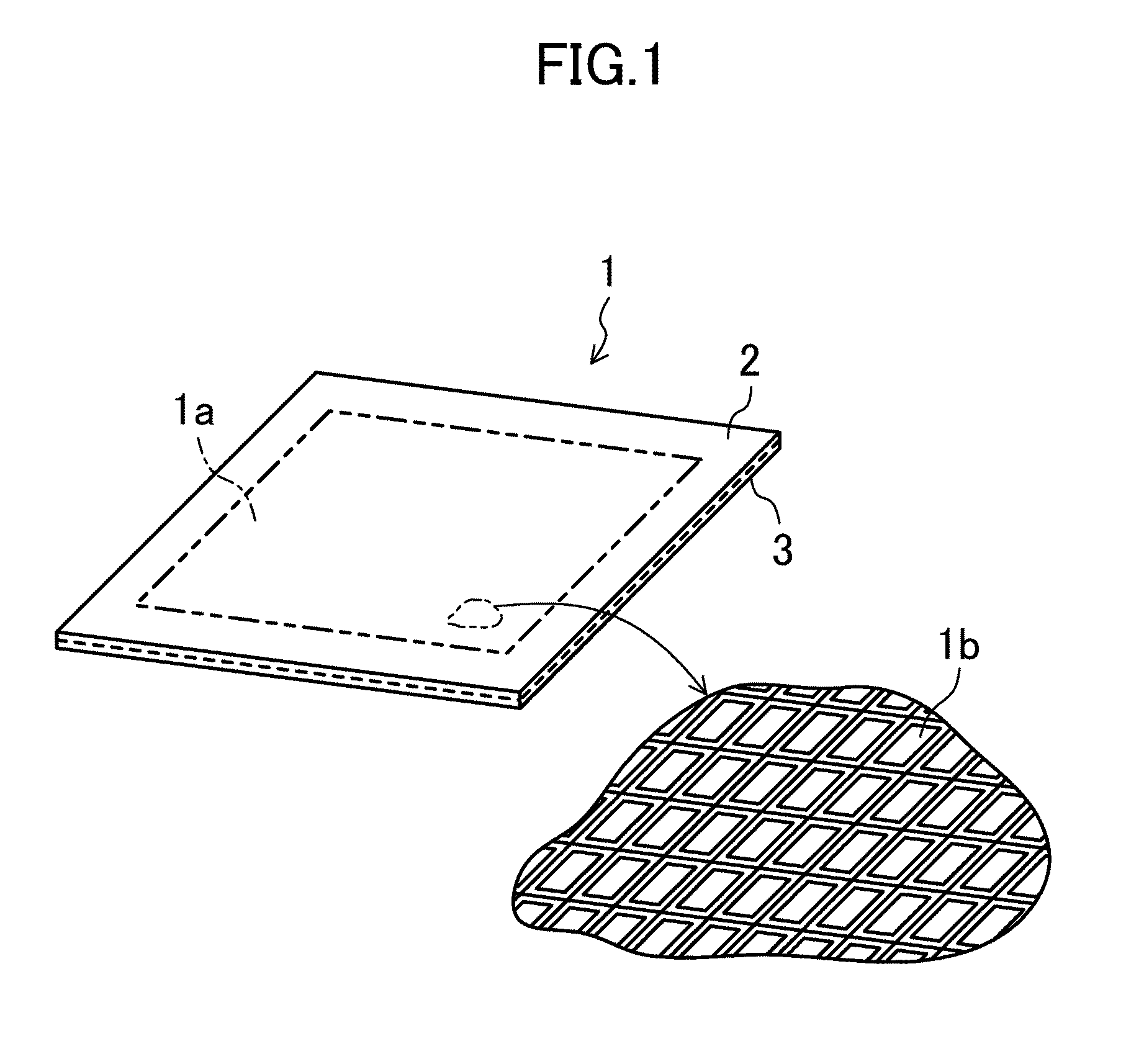
[0081]FIG. 1 shows a panel 1 of a liquid crystal display (display device) according to this embodiment to which the present invention is applied. The liquid crystal display is a color display which can display moving images. A plurality of pixels are arranged in a matrix in a display region 1a of the panel 1. Note that the present invention is not limited to liquid crystal displays and is applicable to organic EL displays.

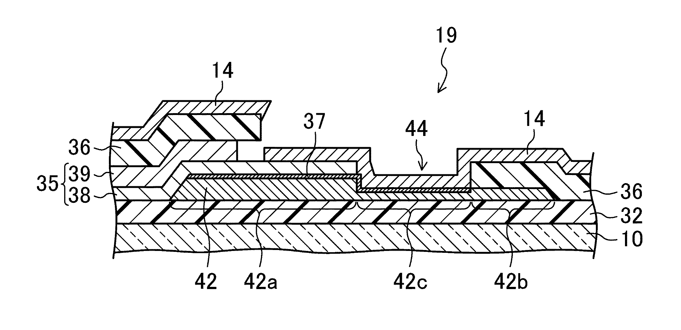
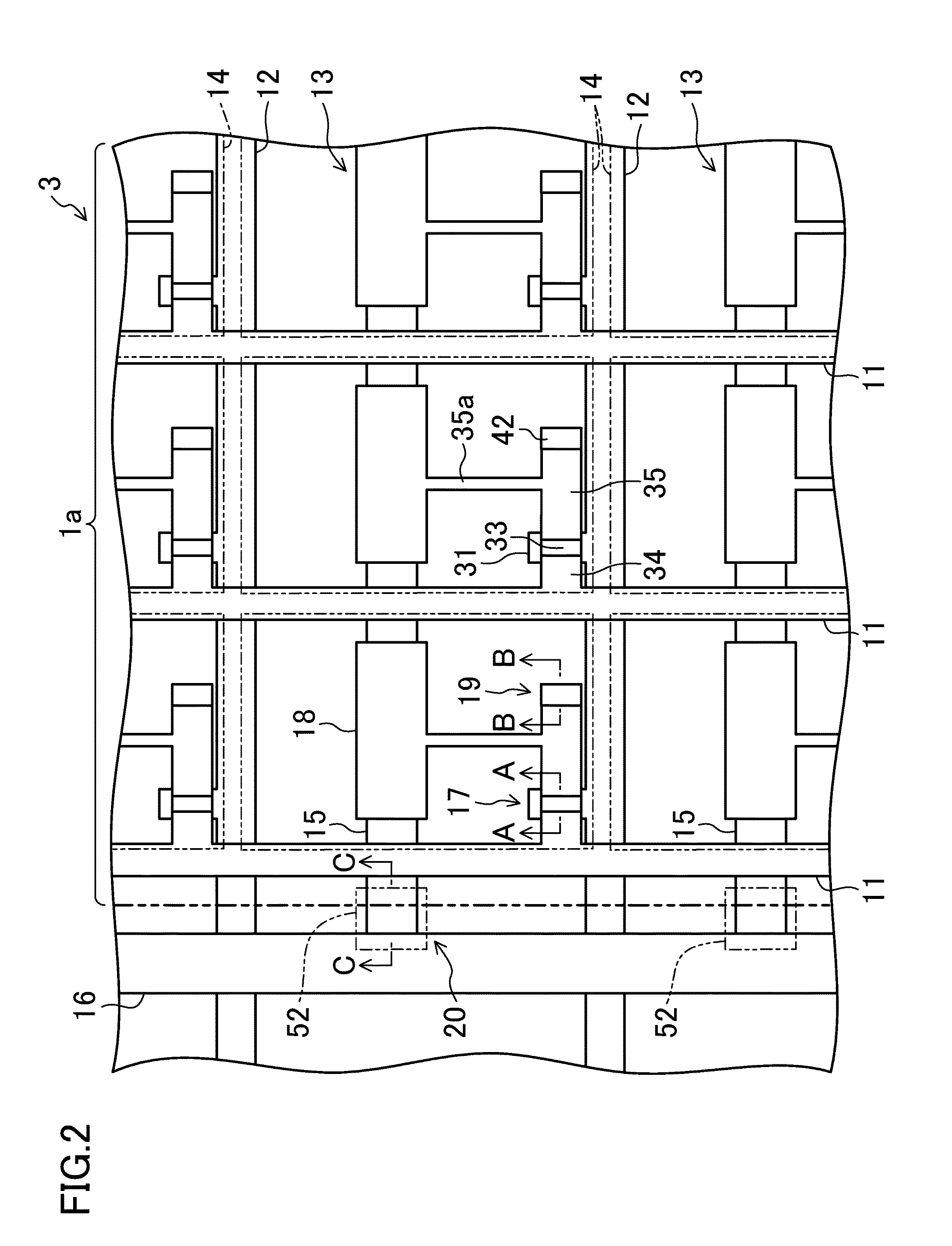
[0082]The panel 1 is formed by bonding a pair of substrates 2 and 3 together with a liquid crystal layer (not shown) being enclosed between the substrates 2 and 3. The substrate 2 is a CF substrate on which red, green, and blue color filters are arranged in a predetermined pattern. The substrate 3 is an active matrix drive type TFT substrate. On the TFT substrate 3, thin film transistors (TFTs 17) and contact structures 19 and 20 are provided by stacking films which are each formed of a conductive or insulating material having a predetermined pattern together...

second embodiment

[0167]This embodiment is different from the first embodiment in that the source electrode 34 etc. are not formed of Al, which is resistant (high selectivity) to fluorine-based gas, and are formed only of another material(s) (metal having a high melting point) which is not resistant (low selectivity) to fluorine-based gas, such as Ti etc. In the description that follows, components different from those of the first embodiment will be described in detail, and components similar to those of the first embodiment are indicated by the same reference characters and will not be described.

[0168]

[0169]FIG. 16 shows a TFT 17 of this embodiment. As shown in FIG. 16, a source electrode 34 and a drain electrode 35 of the TFT 17 are formed only of Ti (i.e., a Ti layer 38). Instead of Ti, other metals, such as tungsten (W), molybdenum (Mo), tantalum (Ta), etc., may be employed.

[0170]

[0171]FIG. 17 shows a first contact structure 19 of this embodiment. As shown in FIG. 17, in a first terminal 42 of t...


PUM


Abstract

A TFT 17 provided on a substrate 3 is provided. The TFT 17 includes a gate electrode 31, a gate insulating film 32, a semiconductor 33, a source electrode 34, a drain electrode 35, and a protection film 36. The semiconductor 33 includes a metal oxide semiconductor. The semiconductor 33 has a source portion 33a which is in contact with the source electrode 34, a drain portion 33b which is in contact with the drain electrode 35, and a channel portion 33c which is exposed through the source electrode 34 and the drain electrode 35. A conductive layer 37 having a relatively small electrical resistance is formed in each of the source portion 33a and the drain portion 33b. The conductive layer 37 is removed from the channel portion 33c.

Description

TECHNICAL FIELD[0001]The present invention relates to display devices, such as a liquid crystal display etc., and more particularly, to thin film transistors, contact structures, etc. including a metal oxide semiconductor which are provided on the substrate of the display device.BACKGROUND ART[0002]In a thin film transistor (TFT) employing a metal oxide semiconductor, an insulating protection layer (etch stopper) is typically formed on the semiconductor layer in order to ensue the reliability of the channel portion. In this case, the source and drain electrodes are connected to the semiconductor layer via two connection holes (contact holes) which are formed in the protection layer.[0003]In the structure, however, it is necessary to highly precisely form the two contact holes with a predetermined clearance, and therefore, it is disadvantageously difficult to provide a high-precision small transistor. It is also disadvantageously difficult to ensure a stable connection using the minu...

Claims


Application Information

Patent Timeline
Patent Type & Authority Patents(United States)
IPC IPC(8): H01L27/105
CPCH01L29/78618H01L27/1225H01L27/1255H01L29/7869H01L29/66969G02F1/136227H01L27/124
Inventor NAKAZAWA, MAKOTO
Owner SHARP KK
Learn More