
Method of forming bank, method of forming film pattern, semiconductor device, electro optic device, and electronic apparatus

a technology of film pattern and bank, which is applied in the direction of photomechanical equipment, instruments, photosensitive material processing, etc., can solve the problems of poor continuity, the developer cannot penetrate the portion to be developed and removed, and the productivity of the development is affected, so as to reduce the lyophobic property and the productivity of the development. , the effect of reducing the lyophobic property

Inactive Publication Date: 2006-11-16
SEIKO EPSON CORP
View PDF1 Cites 9 Cited by
  • Summary
  • Abstract
  • Description
  • Claims
  • Application Information

AI Technical Summary

Benefits of technology

[0012] An advantage of the invention is to provide a method of forming a bank that solves a disadvantage caused by a lyophobic treatment of the bank without impairing the productivity, a method of forming a film pattern using the obtained bank, and further a method of manufacturing a semiconductor device, an electro optic device, and an electronic apparatus.
[0013] A method of forming a bank according to one aspect of the invention is a method of forming a bank that partitions a region for forming a film pattern made of a functional liquid. The method includes: forming a bank film made of a photo resist by applying a photo resist liquid onto a substrate and drying the photo resist liquid, performing a lyophobic treatment for the bank film by using a lyophobic treatment gas and plasma; reducing the lyophobic property by selectively applying UV rays to the bank film after the lyophobic treatment with a mask; selectively exposing the bank film after the lyophobic treatment to light with the mask; developing and patterning the bank film after reducing the lyophobic property and exposing the bank film to light so as to form the bank; wherein the lyophobic property is reduced and the bank film is exposed to light continuously or at the same time with the same mask.
[0014] According to this method of forming a bank, the lyophobic property of a desired portion, namely, a portion to be removed by developing is reduced by exposure to ultraviolet (UV) radiation before developing, and therefore, in developing, the surface of the portion is easily wetted by a developer and the developer penetrates into the portion, since the method includes a process of reducing the lyophobic property by selectively applying UV rays to the bank film after the lyophobic treatment with a mask, a process of selectively exposing the bank film after the lyophobic treatment to light with the mask, and a process of developing and patterning the bank film after reducing the lyophobic property and exposing the bank film to light so as to form the bank. Accordingly, the portion to be removed is reliably removed by developing. Thus, this method secures good pattern accuracy of the bank as well as prevents a disadvantage of the residue remaining in the concave section.
[0015] It is unnecessary to remove or change a mask between the process of reducing the lyophobic property and the process of exposure to light since these processes are performed continuously or at the same time with the same mask. Thus, productivity can be improved.
[0016] In the above method of forming a bank, it is preferable to perform the process of expose to light after the process of reducing the lyophobic property if these processes are continuously performed with the same mask.
[0017] Performing the process of reducing lyophobic property before the process of exposure to light can further improve lyophobic property compared to performing the process of reducing lyophobic property after the process of exposure to light.

Problems solved by technology

In this case, however, when the bank material is exposed to light and developed for patterning, a developer does not sufficiently penetrate the portion to be developed and removed since the property of the surface of the bank material has been modified into being lyophobic.
In particular, a problem is raised if the bank is formed for forming a wiring pattern of the upper layer, which is deposited as a second or higher layer, and a contact hole is formed between the wiring pattern of the upper layer and the conductive section of the lower layer to establish continuity between them.
This may result in poor continuity.

Method used


Image

  • Method of forming bank, method of forming film pattern, semiconductor device, electro optic device, and electronic apparatus
  • Method of forming bank, method of forming film pattern, semiconductor device, electro optic device, and electronic apparatus
  • Method of forming bank, method of forming film pattern, semiconductor device, electro optic device, and electronic apparatus

Examples


first embodiment

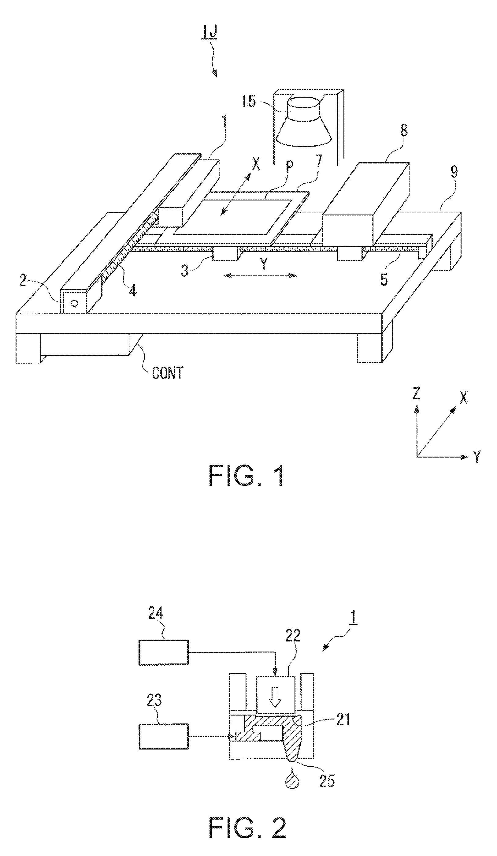
[0054] First an embodiment in which ink (functional liquid) for wiring pattern (film pattern) containing conductive micro particles is discharged as droplets from a nozzle of a droplet discharging head by a droplet discharging method so as to form a wiring pattern (film pattern) in a concave section, namely in a region partitioned by the banks, formed on a substrate corresponding to the wiring pattern, as the method of forming a film pattern according to one embodiment of the invention, will now be described.

[0055] Here, as the ink (functional liquid) for wiring pattern, a dispersion liquid containing conductive micro particles dispersed in a dispersion medium is used. In this embodiment, as conductive micro particles, metal micro particles containing at least one of gold, silver, copper, aluminum, chromium, manganese, molybdenum, titan, palladium, tungsten, and nickel, these oxides, and micro particles of conductive polymers and superconductors are used. The surface of these condu...

second embodiment

[0113] Next, another embodiment in which the method of forming a film pattern according to one embodiment of the invention is applied to a method of forming a wiring pattern (film pattern) will be described.

[0114] This embodiment differs from the above embodiment in that the exposure to UV radiation (process of UV irradiation) shown in FIG. 5C and the exposure to light (process of exposure to light) shown in FIG. 5D are performed at the same time.

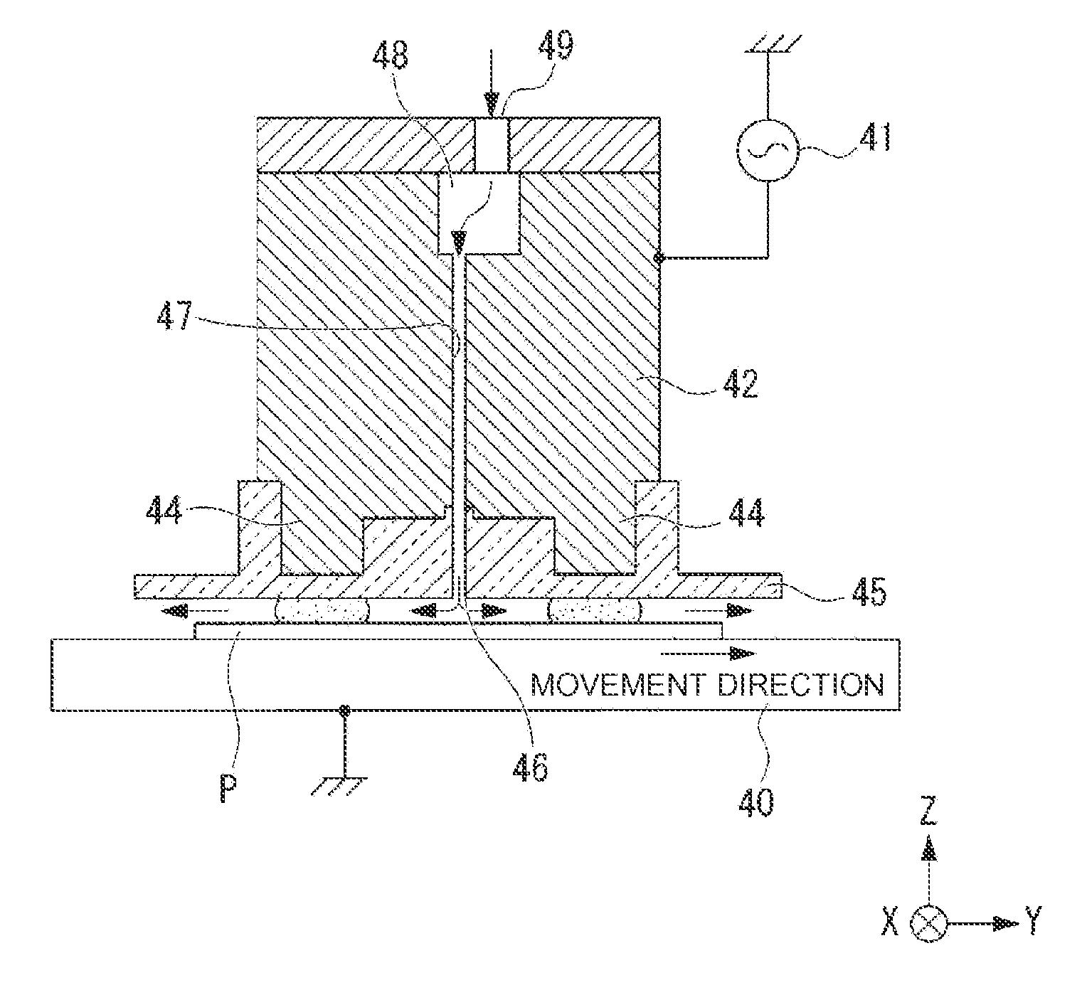
[0115] Namely, in the embodiment, a lyophobic treatment is applied to the surface of the bank film 31 to form the lyophobic layer 37 on the surface as shown in FIG. 5B, and thereafter the exposure to UV radiation and the exposure to light are performed at the same time using the single mask M as shown in FIG. 9. In simultaneous performing, a device having exposure light source for emitting light such as G line (254 nm), H line (365 nm), or I line (405 nm) and another light source for emitting UV rays in the short wavelength region having ...

third embodiment

[0120] Next, another embodiment according to the method of forming a film pattern of the embodiment of the invention will be described. In the embodiment, circuit wiring (wiring pattern) is formed on the wiring pattern (film pattern) formed in the first or second embodiment. A droplet discharging method and a droplet discharging device, and further a semiconductor device manufactured in this embodiment are basically identical to those in the first embodiment.

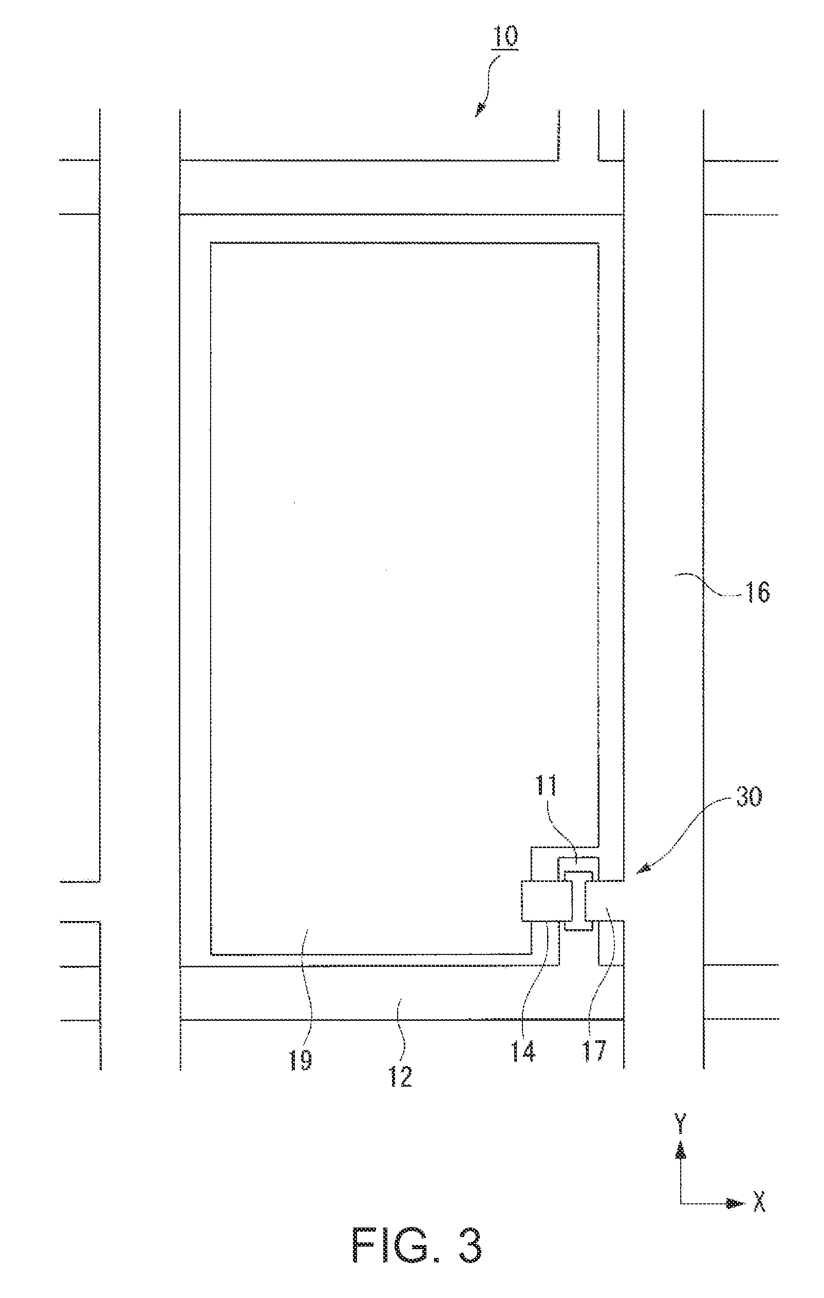
[0121] In the embodiment, first, a gate insulating film (the insulating film 28), an active layer 63, which is a semiconductor film, and a junction layer 64 are continuously formed on the gate wiring 12 (the gate electrode 11) as the wiring pattern formed in the first and second embodiments by a plasama CVD method, as shown in FIG. 10A. A silicon nitride film as the insulating film 28, an amorphous silicon film as the active layer 63, and n+ type silicon film as the junction layer 64 are formed by changing the gas as raw materi...


PUM


Abstract

A method of forming a bank that partitions a region for forming a film pattern made of a functional liquid, includes: forming a bank film made of a photo resist by applying a photo resist liquid onto a substrate and drying the photo resist liquid; performing a lyophobic treatment for the bank film by using a lyophobic treatment gas and plasma; reducing a lyophobic property by selectively applying ultraviolet rays to the bank film after the lyophobic treatment with a mask; selectively exposing the bank film after the lyophobic treatment to light with the mask; developing and patterning the bank film after reducing the lyophobic property and exposing the bank film to light so as to form the bank; wherein the lyophobic property is reduced and the bank film is exposed to light continuously or at the same time with the same mask.

Description

BACKGROUND OF THE INVENTION [0001] 1. Technical Field [0002] The present invention relates to a method of forming a bank, a method of forming a film pattern, a semiconductor device, an electro optic device, and an electronic apparatus. [0003] 2. Related Art [0004] A semiconductor device including circuit wiring to which a thin film (film pattern) made of a conductor is provided, a thin film such as an insulating film that covers the circuit wiring, and a thin film made of a semiconductor, which are stacked on a substrate, are known heretofore. As an efficient method of forming a thin film in such a semiconductor device, a droplet discharging method (inkjet method) according to JP-A-11-274671 is known. In this method, droplets of a functional liquid including a thin film material as dispersoid are discharged from a droplet discharging head, and the functional liquid that has landed is dried for removing the dispersion medium from it, so that a thin film is formed. [0005] If a thin fi...

Claims


Application Information

Patent Timeline
Patent Type & Authority Applications(United States)
IPC IPC(8): H01J17/02
CPCG02F2001/136295G03F7/0045G03F7/0757H01L51/0005G03F7/40H01L27/3244H01L27/3295G03F7/168G02F1/136295H10K59/122H10K71/135H01L21/31144H10K59/12
Inventor MORIYA, KATSUYUKIHIRAI, TOSHIMITSU
Owner SEIKO EPSON CORP
Learn More