Double-active-layer structure with a polysilicon layer and a microcrystalline silicon layer, method for manufacturing the same and its application

a polysilicon and microcrystalline silicon technology, applied in the field of thin film transistor display, can solve the problems of poor illumination uniformity of oled display, affecting the current density flowing through, and the improvement of such methods is only modest, so as to reduce the interference of laser light between a lower amorphous silicon layer and an underlying buffer layer, and achieve the effect of reducing the interference fringe of laser ligh

Inactive Publication Date: 2009-08-06
INNOLUX CORP
View PDF4 Cites 12 Cited by
  • Summary
  • Abstract
  • Description
  • Claims
  • Application Information

AI Technical Summary

Benefits of technology

[0005]An objective of the present invention is to provide a double-active-layer structure with a polysilicon layer and a microcrystalline silicon layer and a method for manufacturing the same, in which two amorphous silicon layers are formed over a substrate, and during a laser annealing process, an upper amorphous silicon layer absorbs more laser light, so that interference of laser light between a lower amorphous silicon layer and an underlying buffer layer is reduced. Accordingly, interference fringes of laser light can be reduced.
[0006]Another objective of the present invention is to provide a double-active-layer structure with a polysilicon layer and a microcrystalline silicon layer to be used in an OLED display, wherein the microcrystalline silicon layer can serve as an active layer of TFTs in the display area to improve illumination uniformity thereof, while the polysilicon layer can serve as an active layer of TFTs in the driving circuit area.
[0009]The TFT display of the present invention can be an OLED display. By forming TFTs having microcrystalline silicon channel regions in the display area, illumination uniformity thereof can be improved.

Problems solved by technology

That is to say, the above ELA process tends to affect the quality of the channel region of subsequently formed TFTs, further affecting the current density flowing through every OLED unit.
This may result in poor illumination uniformity of the OLED display.
However, the improvement brought by such method is only modest.

Method used


Image

  • Double-active-layer structure with a polysilicon layer and a microcrystalline silicon layer, method for manufacturing the same and its application
  • Double-active-layer structure with a polysilicon layer and a microcrystalline silicon layer, method for manufacturing the same and its application
  • Double-active-layer structure with a polysilicon layer and a microcrystalline silicon layer, method for manufacturing the same and its application

Examples


Embodiment Construction

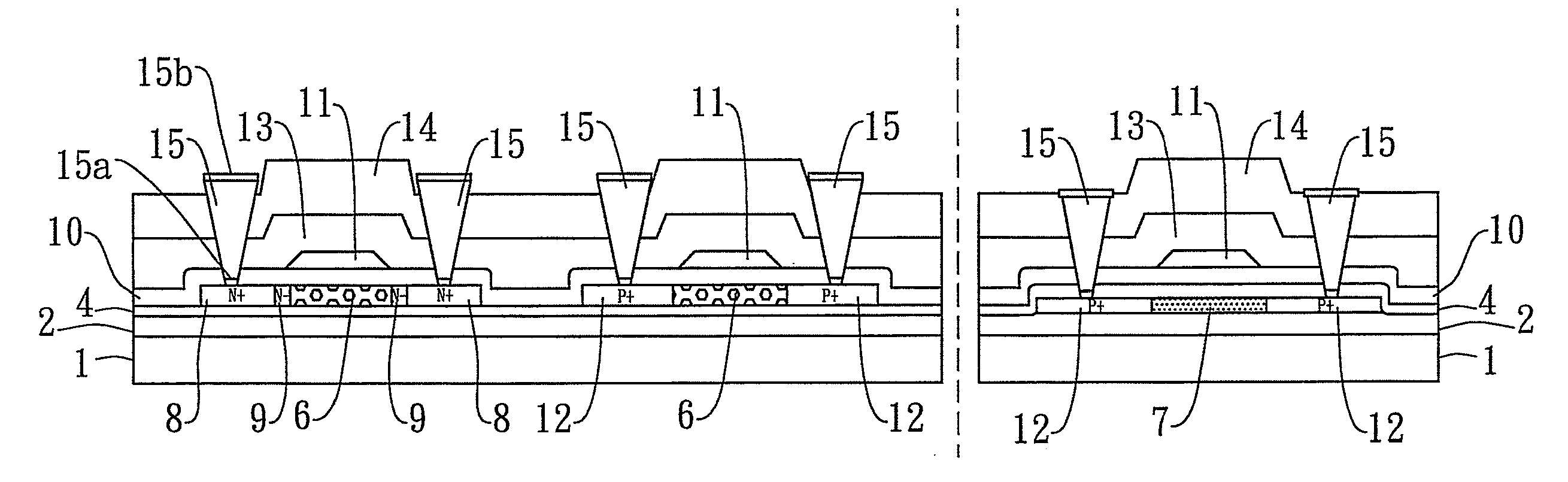
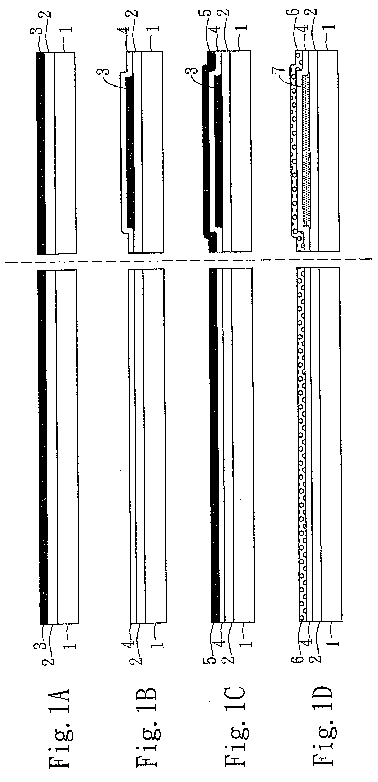
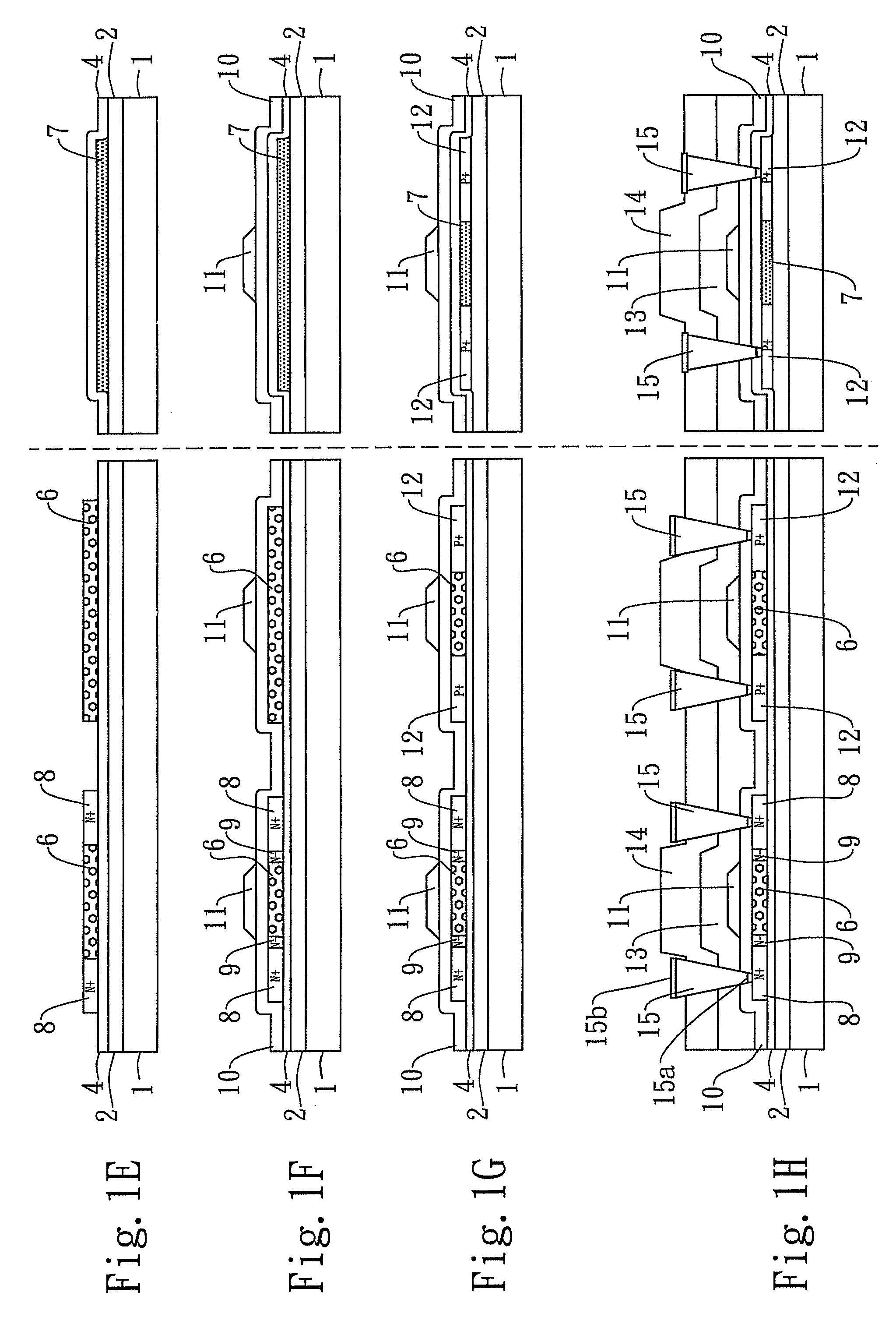
[0012]FIGS. 1A through 1D are schematic cross-sectional views respectively corresponding to various stages of manufacturing a double-active-layer structure with a polysilicon layer and a microcrystalline silicon layer of the present invention. Referring to FIG. 1A, a substrate 1, such as a glass substrate or other semiconductor substrate, is provided first. A display area is defined on the right side surface of the substrate 1, and a driving circuit area is defined on the left side surface thereof. A buffer layer 2 is formed over the substrate 1, and next, a first amorphous silicon layer 3 is formed over the buffer layer 2. Referring to FIG. 1B, by patterning the first amorphous silicon layer 3, a first active layer is formed in the display area on the substrate 1. The first active layer includes the patterning first amorphous silicon layer 3. A first insulating layer 4 is then formed over the first active layer, and over the part of the substrate 1 that is not covered by the first ...


PUM


Abstract

A first amorphous silicon layer is formed over a substrate and a second amorphous silicon layer is formed over the first amorphous silicon layer. When a laser annealing process is performed, the second amorphous silicon layer absorbs more laser light than the first amorphous silicon layer does. The first amorphous silicon layer crystallizes into a microcrystalline silicon layer and the second amorphous silicon layer crystallizes into a polysilicon layer. During the laser annealing process, light interference between the first amorphous silicon layer and an underlying buffer layer is eliminated owing to that the second amorphous silicon layer absorbs more laser light. The laser fringe is eliminated. The microcrystalline silicon layer with better crystalline uniformity can serve as an active layer for TFTs in the display area of an OLED display to improve its illumination uniformity.

Description

BACKGROUND OF THE INVENTION[0001]1. Field of the Invention[0002]The present invention relates to a thin film transistor (TFT) display and to a method for manufacturing the same; more particularly, the present invention relates to a TFT display having a double-active-layer structure with a polysilicon layer and a microcrystalline silicon layer, and to a method for manufacturing the same.[0003]2. Description of the Related Art[0004]In a conventional method for manufacturing an organic light-emitting diode (OLED) display, a buffer layer is usually formed over a substrate prior to the deposition of an amorphous silicon active layer. This advance step is to prevent the impurities in the glass substrate from diffusing into the active layer during the subsequent excimer laser annealing (ELA) process, by which an amorphous silicon active layer can crystallize into a polysilicon active layer. When long-wavelength laser of a wavelength longer than 400 nm is used in the ELA process, the laser ...

Claims


Application Information

Patent Timeline
Patent Type & Authority Applications(United States)
IPC IPC(8): H01L33/00H01L21/20G09F9/00G09F9/30H01L21/336H01L27/32H01L29/786
CPCH01L27/1229H01L27/1237H01L29/4908H01L21/02675H01L21/02532H01L21/02595H01L29/78621H01L27/1296
Inventor LIU, HANSONLEE, RYAN
Owner INNOLUX CORP
Why Eureka
Try Eureka