El display device

a display device and display technology, applied in static indicating devices, electroluminescent light sources, instruments, etc., can solve problems such as display non-uniformity and display image quality degradation

Inactive Publication Date: 2009-08-13
TOSHIBA MATSUSHITA DISPLAY TECH
View PDF20 Cites 164 Cited by
  • Summary
  • Abstract
  • Description
  • Claims
  • Application Information

AI Technical Summary

Benefits of technology

[0011]The present invention can provide a sufficient offset cancel period, and therefore enables the drive transistor to be desirably offset canceled. It is therefore possible to compensate for the characteristic variation of the drive transistor, making it possible to realize an image display having no characteristic display nonuniformity.

Problems solved by technology

A drawback of the organic EL element, however, is that display nonuniformity occurs when there is variation in the transistor characteristics of the polysilicon transistor array.
The variation in the characteristic of the drive transistor therefore appears as display nonuniformity and degrades display image quality.

Method used


Image

  • El display device
  • El display device
  • El display device

Examples


first embodiment

[0145]The following describes the First Embodiment of the present invention.

[0146]It should be noted that, in the drawings, the portions and components irrelevant to the description are omitted. As such, the elements illustrated in a particular figures can be applied to or combined with other figures even when the elements are not illustrated in these figures. Further, the figures contain portions or components that are enlarged or reduced for illustrative purposes. Note also that the First through Seventh Embodiments below may be combined.

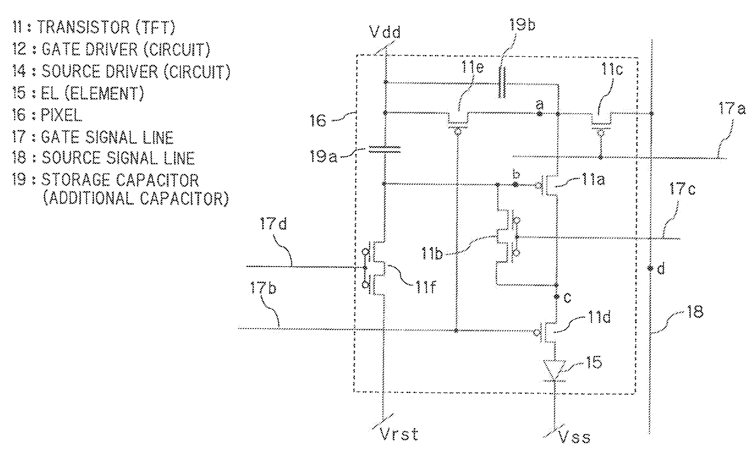
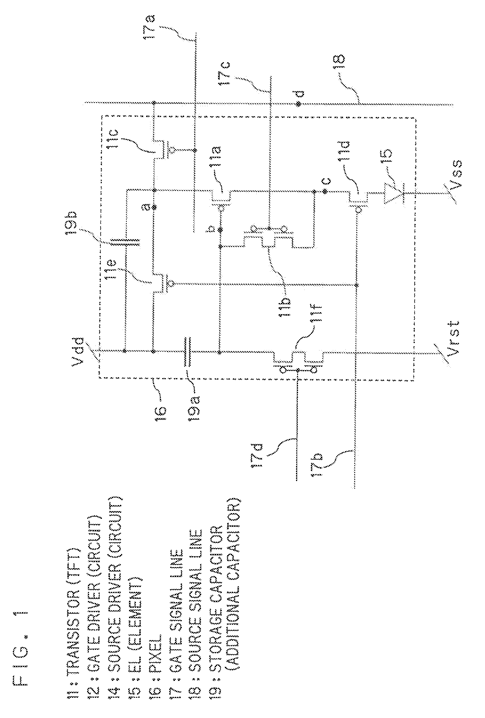
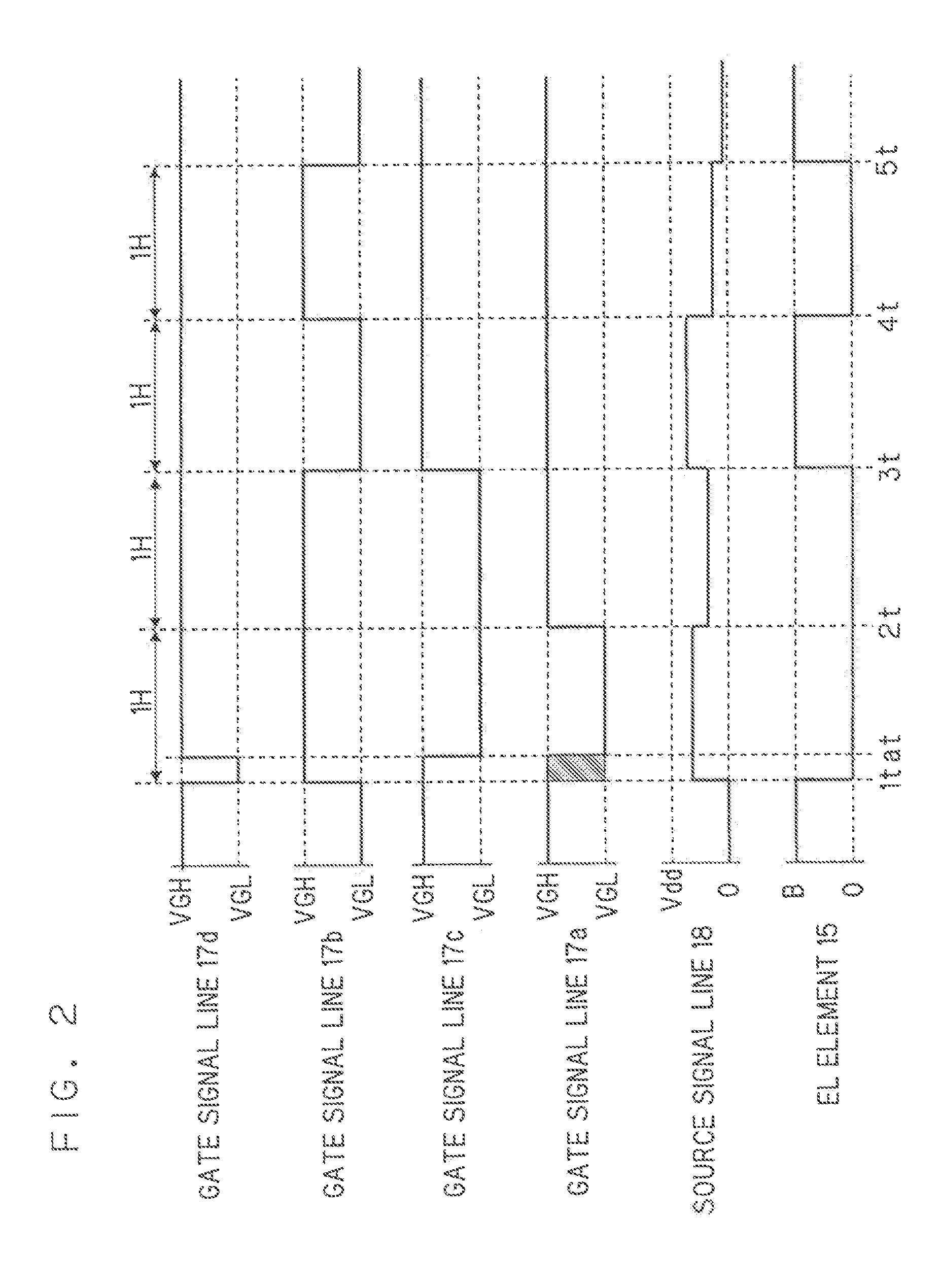
[0147]FIG. 1 depicts a pixel configuration of an EL display device of the First Embodiment. FIG. 3 is a configuration in which a gate driver circuit 12 and a source driver circuit IC 14 are connected to a display region 31 that includes pixels 16 disposed in a matrix.

[0148]As illustrated in FIG. 3, the gate driver circuit 12 receives a clock signal (CLK), start signals (ST1, ST2), and an up-down signal (UP). The clock signal (CLK) is in synchronis...

second embodiment

[0303]The following will describe the Second Embodiment of the present invention.

[0304]FIG. 114 is a block diagram illustrating the overall structure of an EL display device of the Second Embodiment.

[0305]In this embodiment, an EL element 15 includes a display screen 31 provided in a matrix format, and driver circuits that drive the display screen 31. More specifically, as illustrated in FIG. 114, the EL display device includes a source driver circuit (IC) 18, gate terminal gate driver circuits 12 and 12c, and the display screen 31 driven by these driver circuits.

[0306]The gate driver circuit 12 shown in FIG. 114 is a combination of the gate driver circuits 12a and 12b of FIG. 113.

[0307]The display screen 31 includes row gate signal lines 17, column source signal lines 18, a pixel 16 disposed at each intersection of the gate signal lines 17 and the source signal lines 18, and an anode power wire 1131 corresponding to each column of the pixels 16. In other words, the anode power wire...

third embodiment

[0402]The following describes the Third Embodiment of the present invention. Note that the structures and schemes described above can be applied to or combined with the structures and schemes described below.

[0403]FIG. 14 illustrates a circuit for one column of an EL display panel of this embodiment. Through switching means 141, the source signal line 18 is divided into a source signal line 18a and a source signal line 18b in each row, and the source signal lines connected to the pixels of the even-numbered rows and the odd-numbered rows are different (also see, for example, FIG. 6).

[0404]Each pixel 16 has the circuit structure of, for example, FIG. 1, FIG. 4, FIG. 10, FIG. 25, FIG. 29, FIG. 42, FIG. 46, FIG. 52, FIG. 54, FIG. 55, FIG. 58, FIG. 59, FIG. 86, FIG. 87, FIG. 90, FIG. 91, FIG. 92, FIG. 93, FIG. 94, FIG. 95, FIG. 113, FIG. 122, and FIG. 124 through FIG. 128. That is, the embodiment described below is applicable to the other embodiments of this specification, or the embodi...


PUM


Abstract

An EL display device includes: a source driver circuit to output a video signal voltage; a gate driver circuit to select a pixel in a display screen; a first capacitor to maintain the video signal voltage; and a drive transistor to supply current to an EL element of a pixel. The video signal voltage is applied to the drive transistor to perform a predetermined operation, and written into the first capacitor. The video signal voltage maintained in the first capacitor is used to perform an offset cancel operation.

Description

BACKGROUND OF THE INVENTION[0001]1. Field of the Invention[0002]The present invention relates to EL display devices (organic light-emitting display devices) using an EL display panel (display device) or other types of self-emitting display panels (display devices) that use an organic or an inorganic electroluminescence (EL) element. The invention also relates to display panels and display devices including a capacitor (storage capacitor, additional capacitor) that maintains a video signal voltage (video signal data) Vsig at a pixel for a predetermined time period.[0003]2. Description of the Related Art[0004]In active-matrix type image display devices using organic electroluminescence (EL) material or inorganic EL material as the electro-optic converting material, the emission luminescence varies according to the current written in pixels. The EL display device is a self-emitting display that includes a light-emitting element for each pixel. The EL display device has a number of adva...

Claims


Application Information

Patent Timeline
Patent Type & Authority Applications(United States)
IPC IPC(8): G09G3/30H05B44/00
CPCG09G3/3233G09G2320/043G09G2300/0819G09G2300/0814H01L21/02576H01L21/02579H10K50/11
Inventor TAKAHARA, HIROSHITSUGE, HITOSHI
Owner TOSHIBA MATSUSHITA DISPLAY TECH
Why Eureka
Try Eureka