Millisecond annealing (DSA) edge protection

a technology of annealing and edge protection, applied in the direction of manufacturing tools, metal-working machine components, large fixed members, etc., can solve the problems of limiting the speed at which one can heat and cool the substrate, the rtp system of today's state of the art cannot achieve a 400° c./s ramp-up rate and a 150° c./s ramp-down ra

Active Publication Date: 2009-08-20
APPLIED MATERIALS INC
View PDF14 Cites 31 Cited by
  • Summary
  • Abstract
  • Description
  • Claims
  • Application Information

AI Technical Summary

Benefits of technology

[0009]Embodiments of the present invention provide an apparatus for processing a substrate in a processing chamber, comprising a substrate support configured to position a substrate for processin

Problems solved by technology

This limits how fast one can heat and cool the substrate.
Moreover, once the entire substrate is at an elevated temperature, heat can only dissipate into the surrounding space or structures.
As a result, today's state of the art RTP systems struggle to achieve a 400° C./s ramp-up rate and a 150° C./s ramp-down rate.
While RTP and spike annealing processes are widely used, current technology is not ideal because it ramps substrate temperature too slowly during thermal processing, exposing the substrate to elevated temperatures for an extended period of time.
These thermal budget problems become more severe with increasing substrate sizes, increasing switching speeds, and/or decreas

Method used


Image

  • Millisecond annealing (DSA) edge protection
  • Millisecond annealing (DSA) edge protection
  • Millisecond annealing (DSA) edge protection

Examples


Embodiment Construction

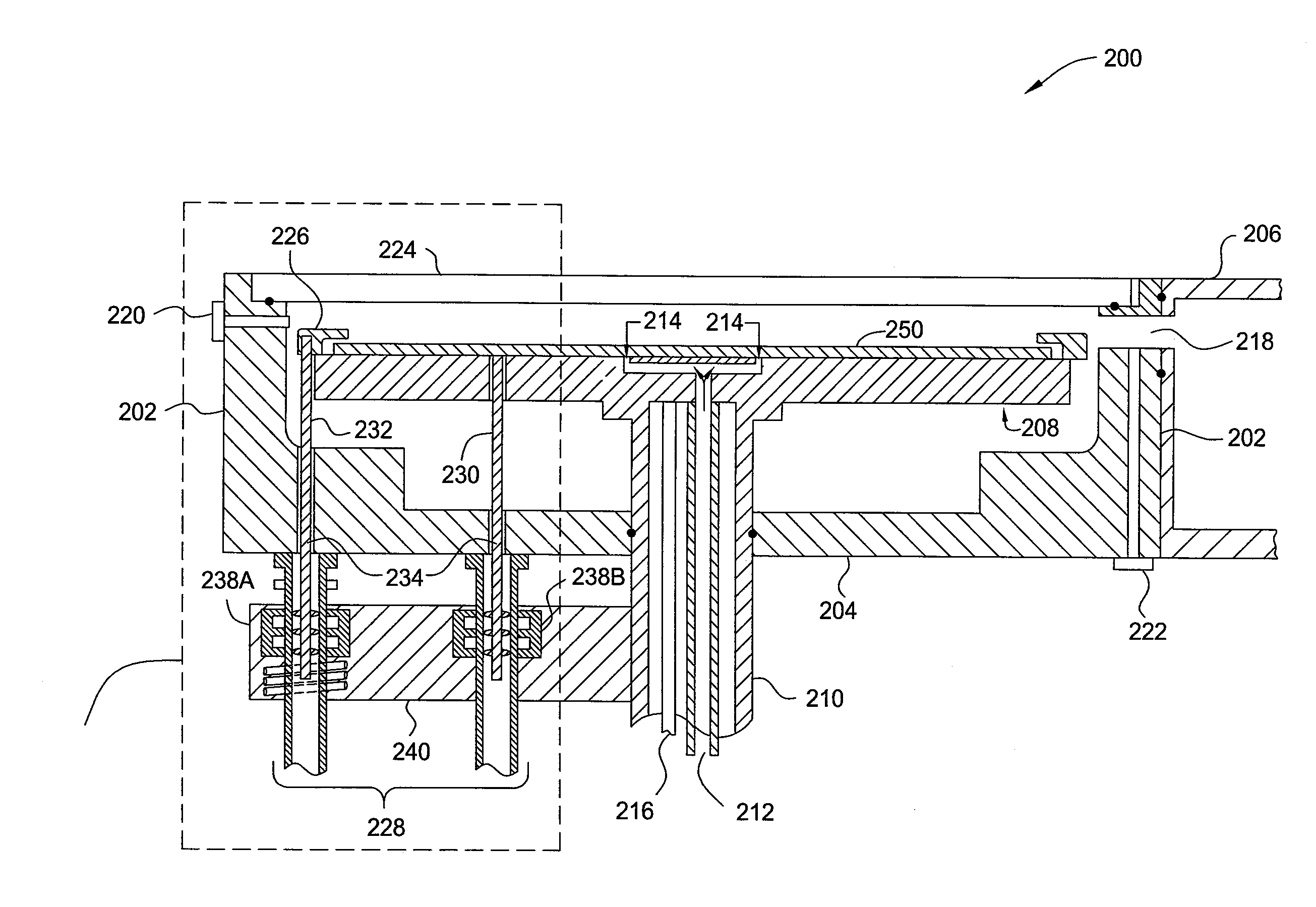
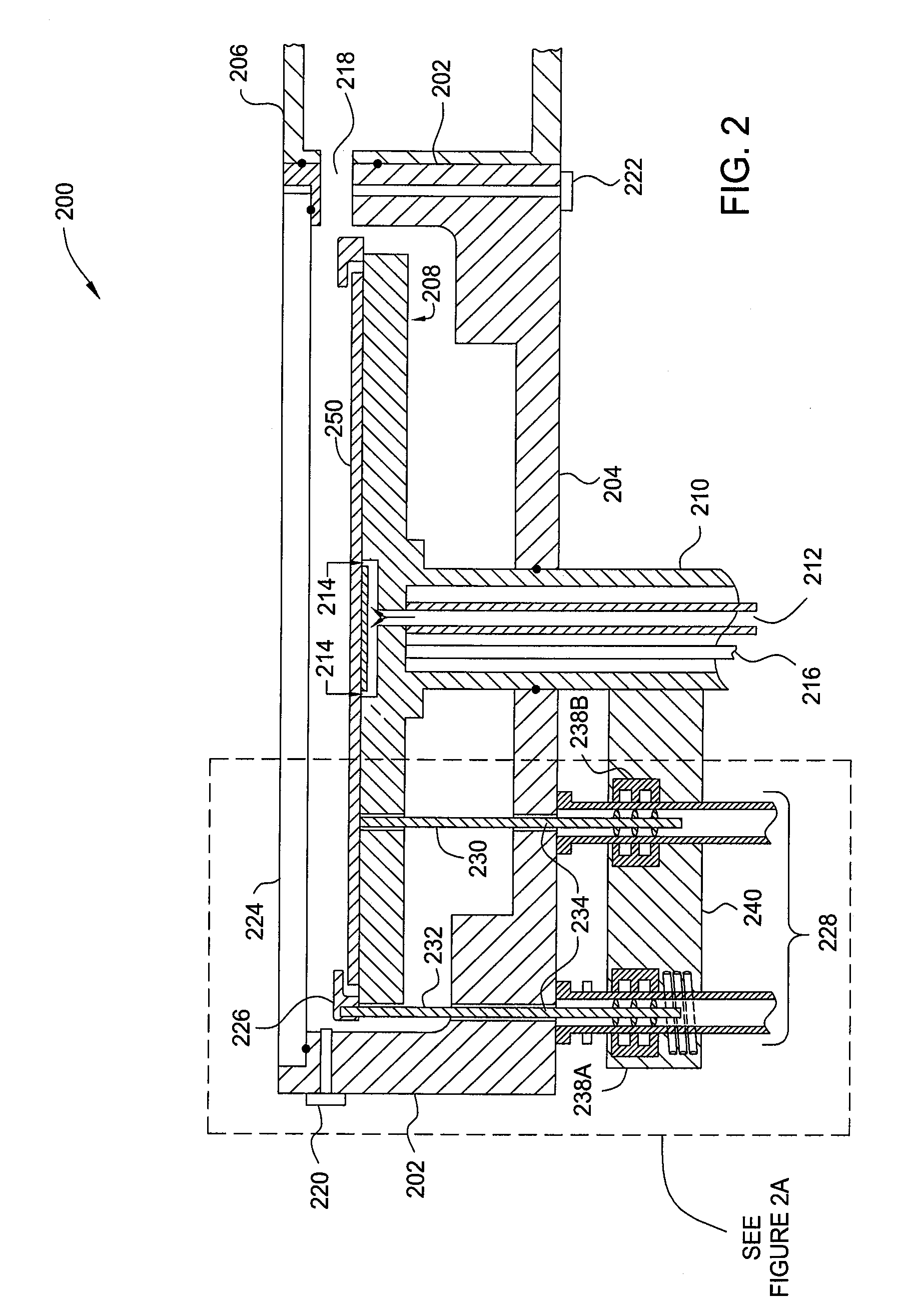
[0022]Embodiments of the present invention provide an apparatus and method for thermal processing of a substrate. In a process chamber configured to perform thermal processes involving directing electromagnetic energy toward at least a portion of the surface of a substrate, a device is deployed to block at least a portion of the electromagnetic energy from reaching the substrate. The device is configured to allow insertion and removal of the substrate by any of several means, and is made to withstand the conditions present during processing of the substrate.

[0023]FIG. 2 is a cross-section view of a thermal processing chamber 200 according to one embodiment of the invention. Chamber 200 features a wall 202, a floor 204, and a top portion 206 cooperatively defining a processing chamber. The processing chamber contains a substrate support 208 for positioning a substrate in the chamber. The substrate support 208 includes a conduit portion 210, which pierces floor 204, for carrying vario...


PUM


Abstract

A method and apparatus for thermally processing a substrate is provided. A substrate is disposed within a processing chamber configured for thermal processing by directing electromagnetic energy toward a surface of the substrate. An energy blocker is provided to block at least a portion of the energy directed toward the substrate. The blocker prevents damage to the substrate from thermal stresses as the incident energy approaches an edge of the substrate.

Description

BACKGROUND OF THE INVENTION[0001]1. Field of the Invention[0002]Embodiments of the present invention generally relate to an apparatus and method for manufacturing a semiconductor device. More particularly, the invention is directed to an apparatus and method for thermally processing a substrate.[0003]2. Description of the Related Art[0004]The integrated circuit (IC) market is continually demanding greater memory capacity, faster switching speeds, and smaller feature sizes. One of the major steps the industry has taken to address these demands is to change from batch processing silicon substrates in large furnaces to single substrate processing in a small chamber.[0005]During single substrate processing, the substrate is typically heated to a high temperature to allow various chemical and physical reactions to take place in multiple IC devices defined in portions of the substrate. Of particular interest, favorable electrical performance of the IC devices requires implanted regions to...

Claims


Application Information

Patent Timeline
IPC IPC(8): H01L21/268B23Q3/00
CPCH01L21/268H01L21/68742H01L21/68735H01L21/67115
Inventor KOELMEL, BLAKEMCINTOSH, ROBERT C.LARMAGNAC, DAVID DLLERNER, ALEXANDER N.MAYUR, ABHILASH J.YUDOVSKY, JOSEPH
Owner APPLIED MATERIALS INC
Why Eureka
Try Eureka