
Supply current based testing of CMOS output stages

a technology of supply current and output stage, which is applied in the direction of electronic circuit testing, measurement devices, instruments, etc., can solve the problems of increasing the number of parallel testing devices, the relative low or high power of the driver, and the increase in the cost of the pin electronics, so as to facilitate the current test of each driver transistor

Inactive Publication Date: 2009-08-27
DIALOG SEMICONDUCTOR GMBH
View PDF15 Cites 3 Cited by
  • Summary
  • Abstract
  • Description
  • Claims
  • Application Information

AI Technical Summary

Benefits of technology

[0012]It is still further an objective of the present invention to use ESD (electrostatic discharge) devices to load down each driver transistor and provide a path for current flowing through the output

Problems solved by technology

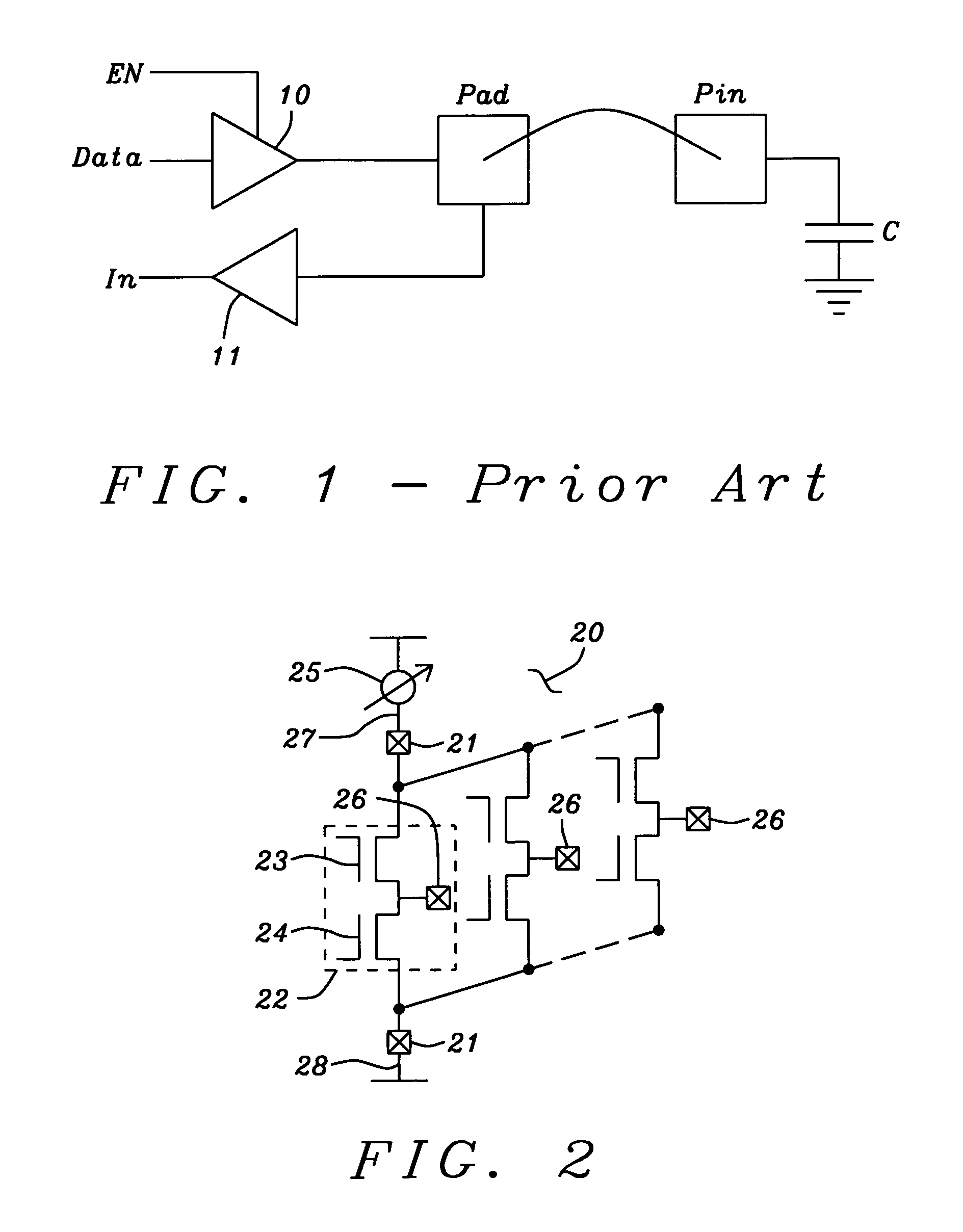
Testing these chips has required testers with many expensive pin electronics to allow the testing of a large variety of chips where input pin on one chip is an output pin on another chip.
Further complicating the requirements of an output pin is that the driver may be relatively low or high power.
Thus the cost of the pin electronics increases as a tester accommodates the variety of possible configurations.
Further as the complexity of the tester increases, the amount of testing devices in parallel becomes limited.
A lower pin count test might leave out DC performance of unconnected pins / pads, which could be acceptable where a second final test after packaging is performed, but is not acceptable for single test insertion devices that are delivered as tested.

Method used


Image

  • Supply current based testing of CMOS output stages
  • Supply current based testing of CMOS output stages
  • Supply current based testing of CMOS output stages

Examples


Embodiment Construction

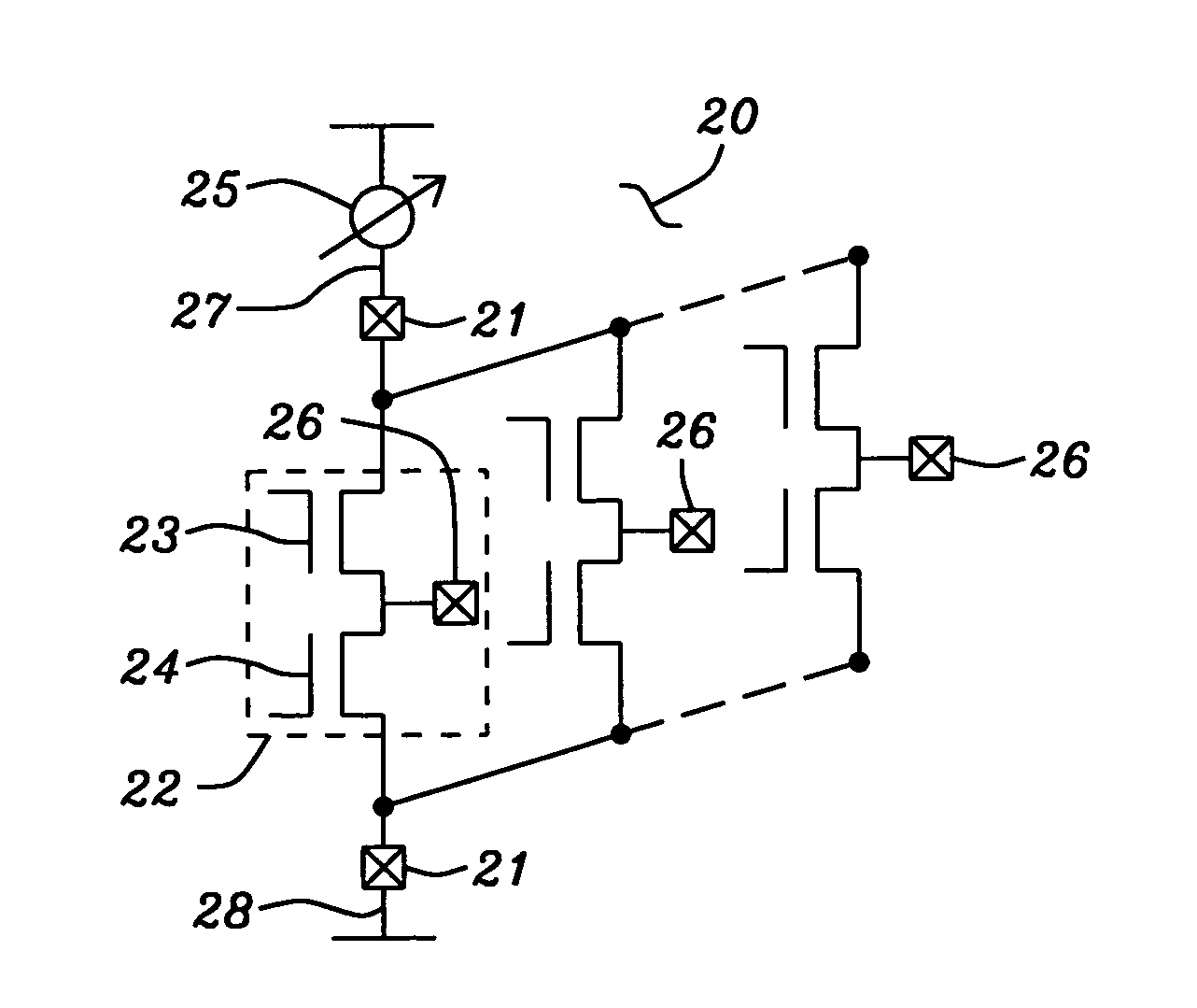
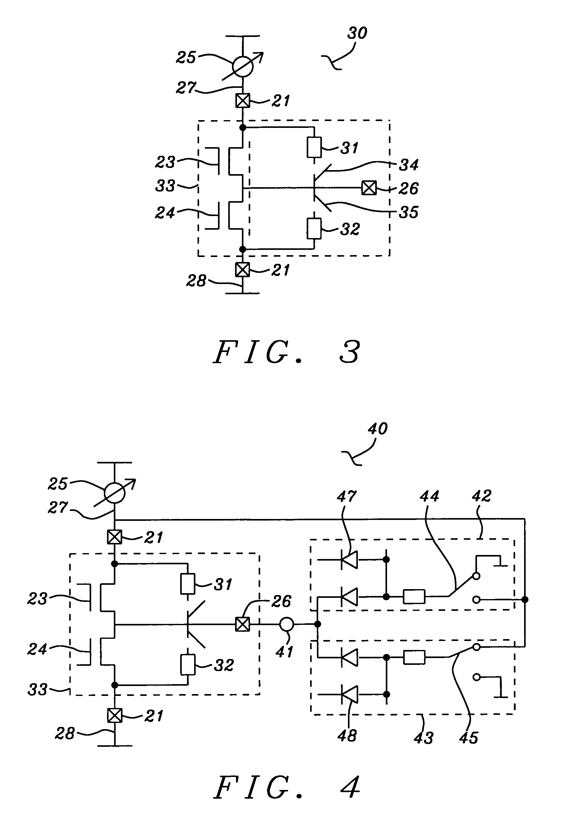
[0022]In FIG. 2 is shown a circuit diagram 20 for leakage testing of transistors forming CMOS driver circuits. Connected between power pads 21 of a semiconductor chip is a plurality of driver circuits 22 connected in parallel. The CMOS driver circuits are formed by a PMOS transistor 23 connected to an NMOS transistor 24 where the connection of the PMOS transistor to the NMOS transistor forms an output connected to an output pad 26 of the chip. A current monitor, or meter, 25 is located in the tester and is connected to a power lead that connects the tester to the chip under test. The current monitor 25 can be located in the tester within either the high voltage power lead 27 or the low voltage power lead 28.

[0023]To measure leakage current, all of the PMOS transistors 23 of the driver circuits connected between the power pads 21 are selected (turned on), and the current monitor 25 measures the leakage current through the NMOS transistors. Then the NMOS transistors 24 are selected (P...


PUM


Abstract

A CMOS driver test configuration, which allows both leakage current and load current testing, using a single monitor, or current meter, located in a power lead of a tester connected to a power pad servicing the driver circuits. Both leakage testing and load current testing for CMOS drivers is described. The test configuration allows a plurality of driver circuits connected in parallel between power pads to be tested simultaneously. An ESD device, internal to the chip, is used as a load during load current testing in chip testing, and an external load is used during package testing in order to include the bonding means between the chip output pad of the driver and the package I / O pin in the current path during load current testing.

Description

BACKGROUND OF THE INVENTION[0001]1. Field of Invention[0002]The present invention is related to testing semiconductor integrated circuit chip and in particular the testing of CMOS driver circuits.[0003]2. Description of Related Art[0004]The evolution of integrated circuit chips has resulted in chips with a higher density of circuits, more I / O pads and a larger variety of functions. Testing these chips has required testers with many expensive pin electronics to allow the testing of a large variety of chips where input pin on one chip is an output pin on another chip. Further complicating the requirements of an output pin is that the driver may be relatively low or high power. Also the driver may operate at a relatively low or high voltage. The driver may be single ended or biased between two voltages. Thus the cost of the pin electronics increases as a tester accommodates the variety of possible configurations. Further as the complexity of the tester increases, the amount of testing ...

Claims


Application Information

Patent Timeline
IPC IPC(8): G01R19/00
CPCG01R31/31924G01R31/3008
Inventor VON STAUDT, HANS MARTINSOMERVILLE, ALAN
Owner DIALOG SEMICONDUCTOR GMBH
Learn More