Illuminating device
- Summary
- Abstract
- Description
- Claims
- Application Information
AI Technical Summary
Benefits of technology
Problems solved by technology
Method used
Image
Examples
first embodiment
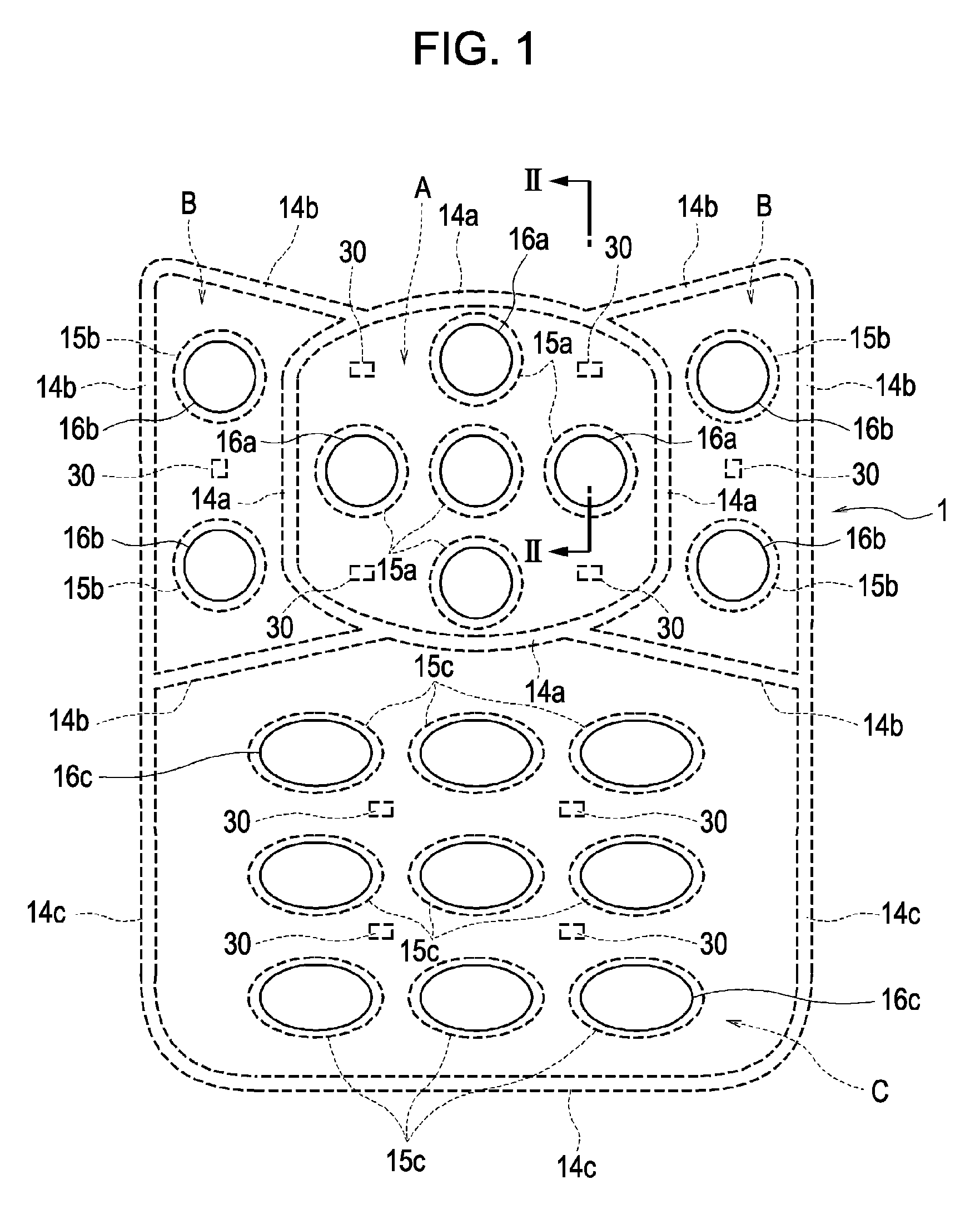
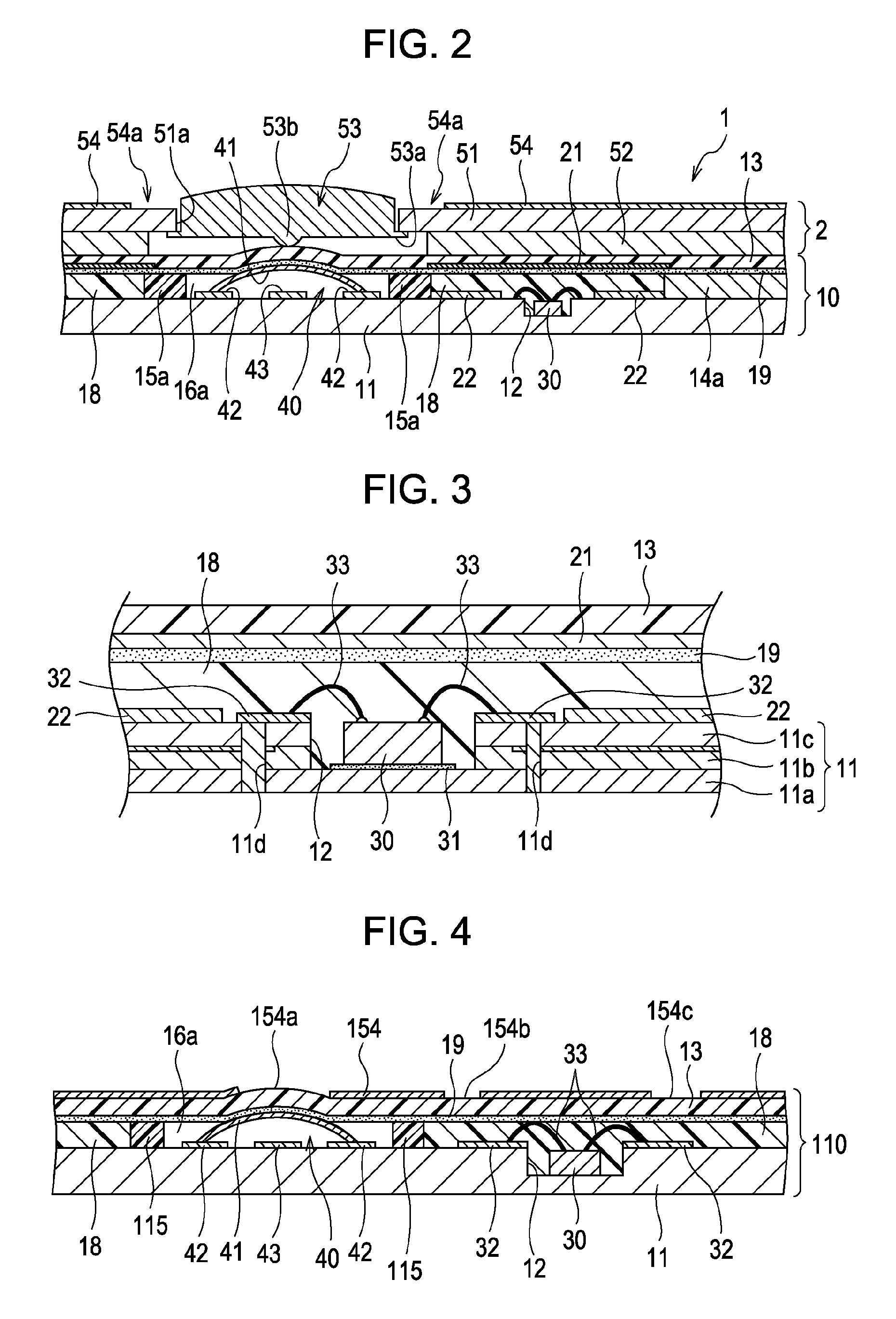
[0037]FIG. 1 is a plan view showing an operation unit 1 that uses an illuminating device according to the present invention. FIG. 2 is a partial cross-sectional view of the operation unit 1 taken along line II-II of FIG. 1. FIG. 3 is a partial enlarged view of FIG. 2.
[0038]The operation unit 1 shown in FIG. 1 is provided to the operation surface of a small electronic apparatus such as a cellular phone. In the operation unit 1, an illumination portion occupying part of the area of the operation unit 1 is lighted up. The apparatus can be operated through a plurality of operation buttons in the operation unit 1.
[0039]For the purposes of this specification, the phrase “light-guiding” used in “light-guiding layer”, “light-guiding property”, etc., refers to the function of an object that allows light to pass through inside. A “light-guiding layer” or a “light-guiding material” means not only a layer or material that is transparent and has a light transmittance of 100% or near, but also a ...
second embodiment
[0082]FIG. 4 is a cross-sectional view showing an illuminating device 110 according to the present invention.
[0083]The illuminating device 110 also has the first sectional boundary layer 14a, the second sectional boundary layers 14b, and the third sectional boundary layer 14c between the substrate 11 and the cover layer 13 to define a plurality of regions A, B, and C. Thus, bare chips 30 that emit light of different hues for different regions can be mounted.
[0084]As shown in FIG. 4, a boundary layer 115 surrounding the mechanism region 16a equipped with the switch mechanism 40 has no light-guiding property and is composed of a non-light-guiding epoxy resin or the like as with the sectional boundary layers 14a, 14b, and 14c. Alternatively, the boundary layer 115 may be composed of a material having a refractive index lower than that of the elastomer 18 so that light propagating in the elastomer 18 can be easily reflected at the interface between the elastomer 18 and the boundary laye...
third embodiment
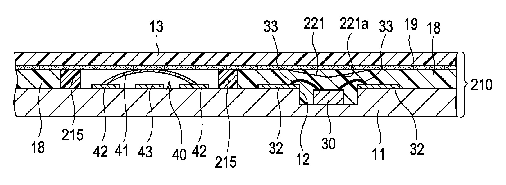
[0089]FIG. 5 is a cross-sectional view showing an illuminating device 210 according to the present invention.
[0090]In this illuminating device 210, a reflector 221 is provided at the lower surface of the cover layer 13 in a portion facing the bare chip 30. The lower surface of the reflector 221 is a reflecting surface 221a sloped with respect to the upper surface of the substrate 11. For example, the reflecting surface 221a is a tapered surface sloped in respective directions. In the cross-sectional view of FIG. 5, the section line of the reflecting surface 221a is straight; however, the section line may be curved outward or curved inward.
[0091]According to the illuminating device 210, light emitted from the bare chips 30 is reflected at the sloped reflecting surface 221a and scattered around within the elastomer 18. A boundary layer 215 surrounding the mechanism region 16a has a higher refractive index than the elastomer 18 and a light-guiding property so that light can be easily g...
PUM
 Abstract
Description
Claims
Application Information


