
Boost converter input ripple current reduction circuit

Inactive Publication Date: 2009-09-17
GENERAL ELECTRIC CO
View PDF24 Cites 10 Cited by
  • Summary
  • Abstract
  • Description
  • Claims
  • Application Information

AI Technical Summary

Benefits of technology

[0005]Briefly, in accordance with one embodiment of the invention, a boost inductor value reduction circuit is configured to substantially reduce the size and inductance value of a boost converter boost inductor that provides a predetermined level of boost converter performance when the boost converter is operating in a continuous conduction mode, such that the reduced inductance boost inductor in combination with the boost inductor value reduction circuit maintains substantially the same predetermined boost converter performance level as that provided by the boost converter operating in the absence of the boost inductor value reduction circuit, and such that the boost converter maintains substantially the same performance level when operating in a continuous conduction mode, in a bounded conduction mode, or in a discontinuous conduction mode.
[0006]According to another embodiment of the invention, a boost inductor value reduction circuit is configured to substantially reduce the size and inductance value of a boost converter boost inductor that is configured to limit a boost converter input ripple current value when the boost converter is operating in a continuous conduction mode, such that the reduced inductance boost inductor in combination with the boost inductor value reduction circuit maintains substantially the same boost converter input ripple current value as that provided by the boost converter operating in the continuous conduction mode in the absence of the boost inductor value reduction circuit, and such that the boost converter maintains substantially the same performance level when operating in a continuous conduction mode, in a bounded conduction mode, or in a discontinuous conduction mode.
[0007]According to yet another embodiment of the invention, a boost inductor value reduction circuit is configured to substantially reduce the size of a boost converter input filter that is operational to limit a boost converter input ripple current value when the boost converter is operating in a continuous conduction mode, such that the reduced size boost converter input filter in combination with the boost inductor value reduction circuit maintains substantially the same boost converter input ripple current value as that provided by the boost converter operating in the continuous conduction mode in the absence of the boost inductor value reduction circuit, and such that the boost converter maintains substantially the same performance level when operating in a continuous conduction mode, in a bounded conduction mode, or in a discontinuous conduction mode.

Problems solved by technology

A significant problem inherent with such boost power converters is related to high frequency harmonics associated with the boost power converter switching frequency fed back to the boost power converter input (i.e. AC power line).
Such techniques, system and devices have generally been very large and expensive since the filtering is required to be very effective at low frequencies (i.e. 100's of kHz).
These filtering techniques often become so large, that the interaction between the filter and boost power converter can create undesirable stability problems.
These filters are large also because all components carry full current.

Method used


Image

  • Boost converter input ripple current reduction circuit
  • Boost converter input ripple current reduction circuit
  • Boost converter input ripple current reduction circuit

Examples


Embodiment Construction

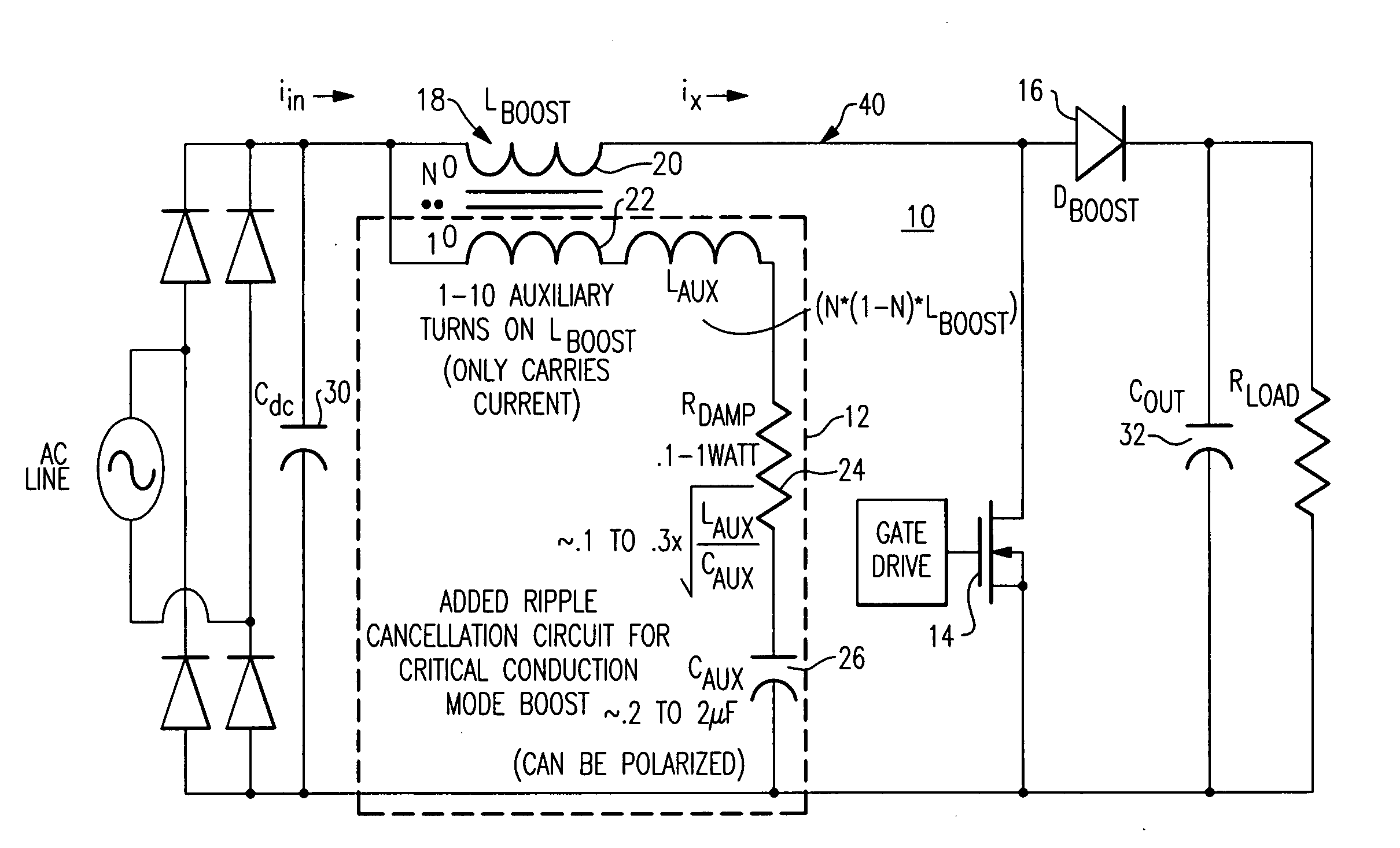
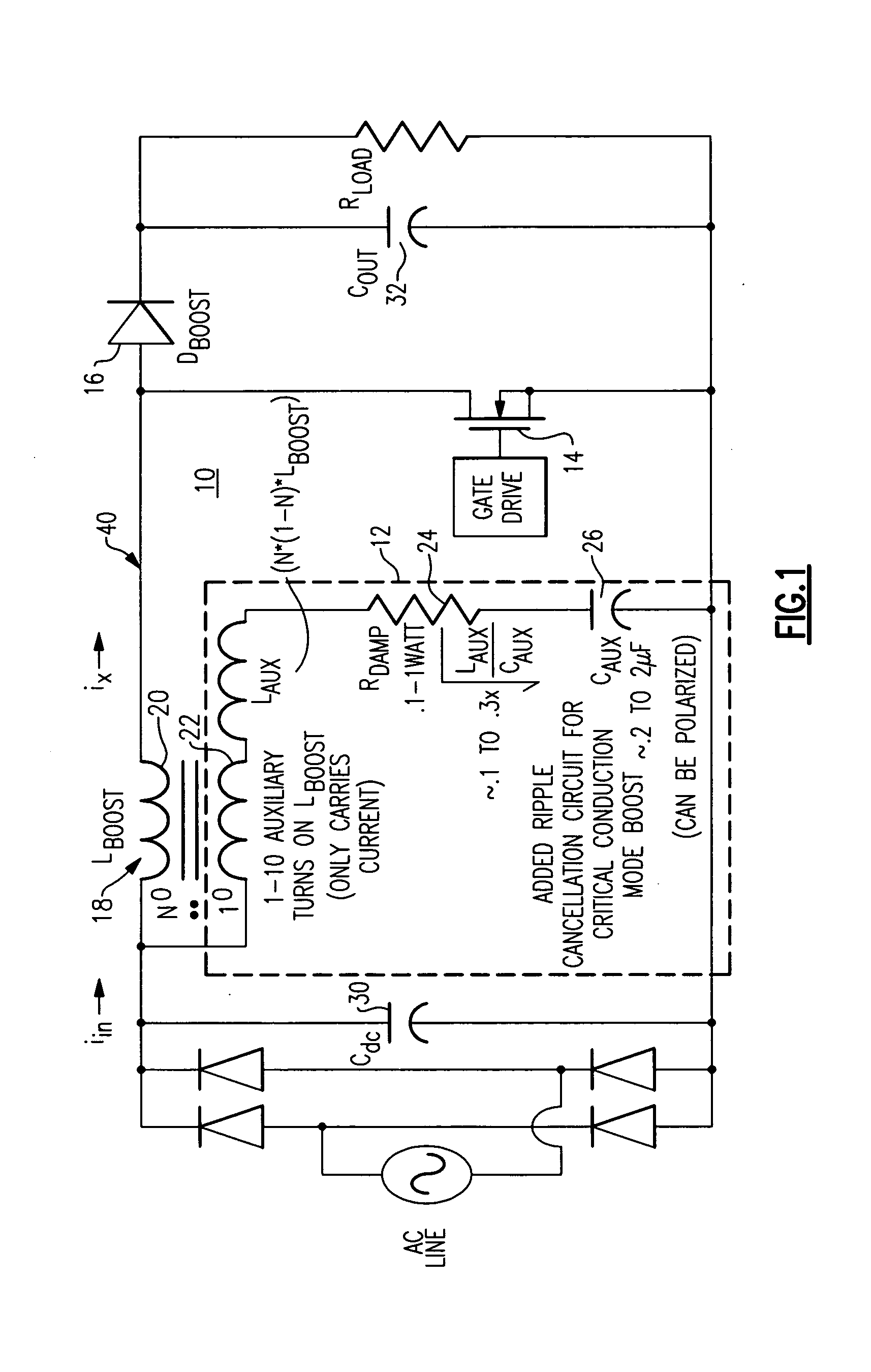
[0016]FIG. 1 illustrates a boost converter 10 including a boost inductor value reduction circuit 12 according to one embodiment of the invention. The boost inductor value reduction circuit 12 is a lightweight, inexpensive and compact ripple cancellation circuit when compared to traditional filter structures. Boost inductor value reduction circuit 12 operates to create a high frequency current signal that substantially cancels the high frequency ripple current conducted back to the AC line input side of the boost converter 10 that is generated by the boost converter 10 switching components. Boost converter 10 switching components can be seen to include a MOSFET 14 and a boost diode 16, according to one embodiment.

[0017]Although boost converter 10 is depicted as having an AC line input, the present embodiments are not so limited; and it shall be understood that the principles described herein apply equally well to a boost converter having a DC input source.

[0018]Boost inductor value r...


PUM


Abstract

A boost inductor value reduction circuit is integrated into a traditional boost power converter to greatly reduce undesirable high frequency harmonics from being fed back to the input side of the boost power converter. The boost inductor value reduction circuit is very small when compared with traditional filter techniques, is less costly than traditional filter techniques, and does not degrade the boost power converter control performance. It can also be used to reduce the size of the boost inductor without compromising the converter performance for use in energy efficient sensitive applications such as photovoltaic inverters.

Description

BACKGROUND[0001]The invention relates generally to boost power converters, and more specifically to a system and method to reduce the input filter size of a boost power converter.[0002]Boost power converters are used in many different applications to provide a high power factor to an AC power line, and / or to provide a regulated DC bus for specific power applications. A significant problem inherent with such boost power converters is related to high frequency harmonics associated with the boost power converter switching frequency fed back to the boost power converter input (i.e. AC power line). These high frequency harmonics are generally required by certain regulatory agencies to be attenuated by factors of 100 or more to meet the requisite regulatory levels. High frequency can also stress capacitors by means of internal heating and dielectric material breakdown.[0003]Known boost power converters have traditionally employed large bulky filtering techniques, systems and devices to re...

Claims


Application Information

Patent Timeline
IPC IPC(8): H02M1/12H02M7/02
CPCH02M1/126Y02E10/56Y02B70/126H02M1/4225Y02B70/10
Inventor SCHUTTEN, MICHAEL JOSEPHSTEIGERWALD, ROBERT LOUISGLASER, JOHN STANLEYSABATE, JUAN ANTONIODE ROOIJ, MICHAEL ANDREW
Owner GENERAL ELECTRIC CO
Learn More