Surface wave excitation plasma processing system

a plasma processing and surface wave technology, applied in plasma technology, energy-based chemical/physical/physico-chemical processes, electric discharge tubes, etc., can solve problems such as failure to obtain uniform plasma, and achieve uniform plasma generation over a large area stably, and prevent interference between adjacent dielectric members

Inactive Publication Date: 2009-09-17
SHIMADZU CORP
View PDF7 Cites 6 Cited by
  • Summary
  • Abstract
  • Description
  • Claims
  • Application Information

AI Technical Summary

Benefits of technology

[0011]According to the present invention, as two or more plasma source parts including a microwave generating part, a microwave waveguide and a dielectric member are disposed, and a reflecting plate is disposed between each of the two dielectric members, so that interferences between the adjacent dielectric members are prevented. Therefore, each plasma generating part can be adjusted independently, so as to maintain a uniform generation of the plasma over a large area stably.

Problems solved by technology

However, in the device described in the Patent Document 1, due to the slight changes of the plasma as a load, the combining status between the microwave power and the plasma of each waveguide is also changed sometimes, such that the distribution ratio of the power input into each waveguide is changed, thus resulting in a failure of obtaining uniform plasma.

Method used


Image

  • Surface wave excitation plasma processing system
  • Surface wave excitation plasma processing system
  • Surface wave excitation plasma processing system

Examples


Embodiment Construction

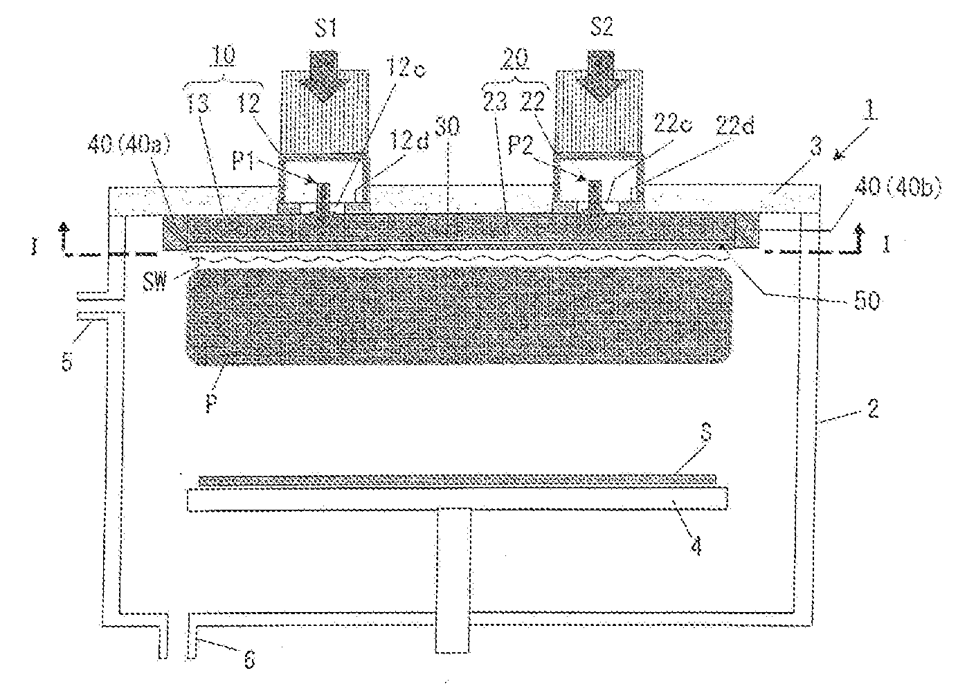
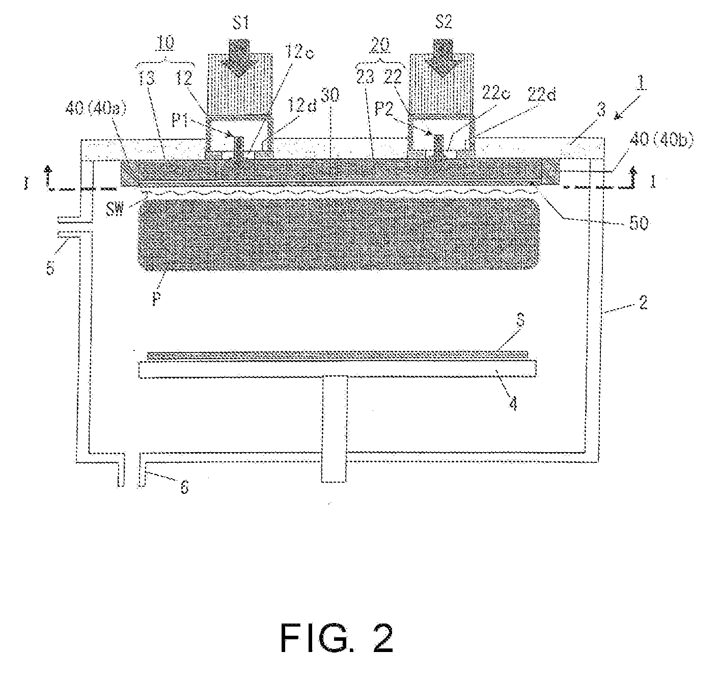
[0019]Hereinafter, a surface wave excitation plasma (SWP: Surface Wave Plasma) processing device (hereinafter briefly referred to as SWP processing device) according to an embodiment of the present invention is illustrated with reference to FIGS. 1-4. FIG. 1 is a plan view schematically showing a general structure of an SWP processing device according to an embodiment of the present invention. FIG. 2 is a cross-sectional view schematically showing structures of the main parts for an SWP processing device according to an embodiment of the present invention.

[0020]Referring to FIGS. 1 and 2, an SWP processing device 100 includes a chamber 1 and two plasma sources 10, 20. The chamber 1 is a sealed frame for performing plasma processing on a substrate to be processed. The plasma source 10 includes a microwave generator 11, a microwave waveguide 12, and a dielectric block 13. The microwave generator 11 has a high voltage power supply 11a, a microwave oscillator 11b, an insulator 11c, a di...


PUM


Abstract

To sustain uniform generation of plasma constantly over a large area. In the surface wave excitation plasma processing device, a plasma source includes: a microwave generator, a microwave waveguide and a dielectric block; and a plasma source also includes: a microwave generator, a microwave waveguide and a dielectric block. The lid of a chamber is fixed onto the microwave waveguides in parallel, and the dielectric blocks disposed in the chamber. A reflecting plate is disposed between the dielectric blocks so that electromagnetic waves propagating through the dielectric blocks are prevented from advancing into the counterpart dielectric blocks as reflected waves. Consequently, the plasma sources are controlled independently. Furthermore, a side reflector is disposed at outer circumference of each of the dielectric blocks so that a standing waves of the electromagnetic waves propagating through the dielectric blocks is formed thus forming a large area standing wave mode of surface waves uniformly.

Description

BACKGROUND OF THE INVENTION[0001]1. Field of the Invention[0002]The present invention relates to a surface wave excitation plasma processing device for performing various treatments by using surface wave excitation plasma.[0003]2. Description of Related Art[0004]As for plasma processing devices capable of generating plasma with high density and over a large area, devices using surface wave excitation plasma are well known. In such devices, it is well known to those skilled in the art that, the microwave waveguide is branched and disposed on a dielectric plate in parallel, such that microwaves guided from a microwave generating part propagate through each microwave waveguide via a plurality of branches, and microwave power is acquired from the dielectric plate in a wider range, thereby realizing a device capable of uniform generation of plasma over a large area (with reference to, for example, Patent Document 1).[0005][Patent Document 1] Japanese Patent Publication No. 2005-33100 (Pa...

Claims


Application Information

Patent Timeline
Patent Type & Authority Applications(United States)
IPC IPC(8): H05H1/46
CPCH05H1/46H01J37/32192
Inventor SUZUKI, MASAYASUSARUWATARI, TETSUYA
Owner SHIMADZU CORP
Why Eureka
Try Eureka