Porous light-emitting compositions

a light-emitting composition and porous technology, applied in the field of light-emitting devices, can solve the problems of reducing quantum yield, reducing extraction efficiency, and reducing efficiency, and achieve the effect of improving light outpu

Inactive Publication Date: 2009-09-17
TRIAD NAT SECURITY LLC
View PDF2 Cites 6 Cited by
  • Summary
  • Abstract
  • Description
  • Claims
  • Application Information

AI Technical Summary

Benefits of technology

[0017]The invention includes new porous light-emitting compositions that are phosphors on three dimensional substrates, and new phosphors based upon coated porous structures. The coated porous structure maintains porosity which may be filled with a liquid, gel, or solid. Filling the cavities with materials of refractive index that match the substrates refractive index can lead to enhanced light output for thick devices such as scintillator based radiation detectors.

Problems solved by technology

Phosphors are an integral part of any LED, and unfortunately contribute significantly to efficiency losses.
The loss mechanisms include fundamental losses innate to the phosphor conversion material (nonradiative decay paths that lead to reduced quantum yields) and reduced extraction efficiency.
One of the major obstacles in the development of high efficiency systems is loss due to wave guiding when thin film phosphors are used.
Porous structures offer great potential, but they are very difficult to coat.
Both of these structures have high surface areas but the nanometer scale porosity with openings or cavities less than 900 nm make them very difficult to coat by traditional line-of-site techniques.
It is not possible to make PCs from just any material, which limits their potential properties.
Coating is one way to add functionality, but traditional techniques Pulsed laser deposition (“PLD”) and Chemical Vapor Deposition (“CVD”) cannot coat the complex porous structures.
ALD is limited in that thicker coatings require many steps and only single component coatings can be readily applied.
However, these crystals have a scintillation decay which is not very fast.
The crystals of the BGO family have high decay time constants, which limit the use of these crystals to low count rates.
However these crystals are very heterogeneous and have very high melting points (about 2200 degrees Celsius).
While thin film scintillators have limited utility in applications where energy resolution is needed in radiation detection, they have major applications in imaging systems such as X-ray imaging device.
One of the prime difficulties in these systems is the gamma-ray rejection characteristics of the system.
In addition, many of the detector materials are air and water sensitive or the scintillators employ heavy elements that limit gamma-ray rejection or have slow response times thanks to the long relaxation times. Scintillators have the added complication that often single crystals are required to avoid light loss, making it difficult to add large amounts of boron or lithium to increase the neutron cross-section absorption.
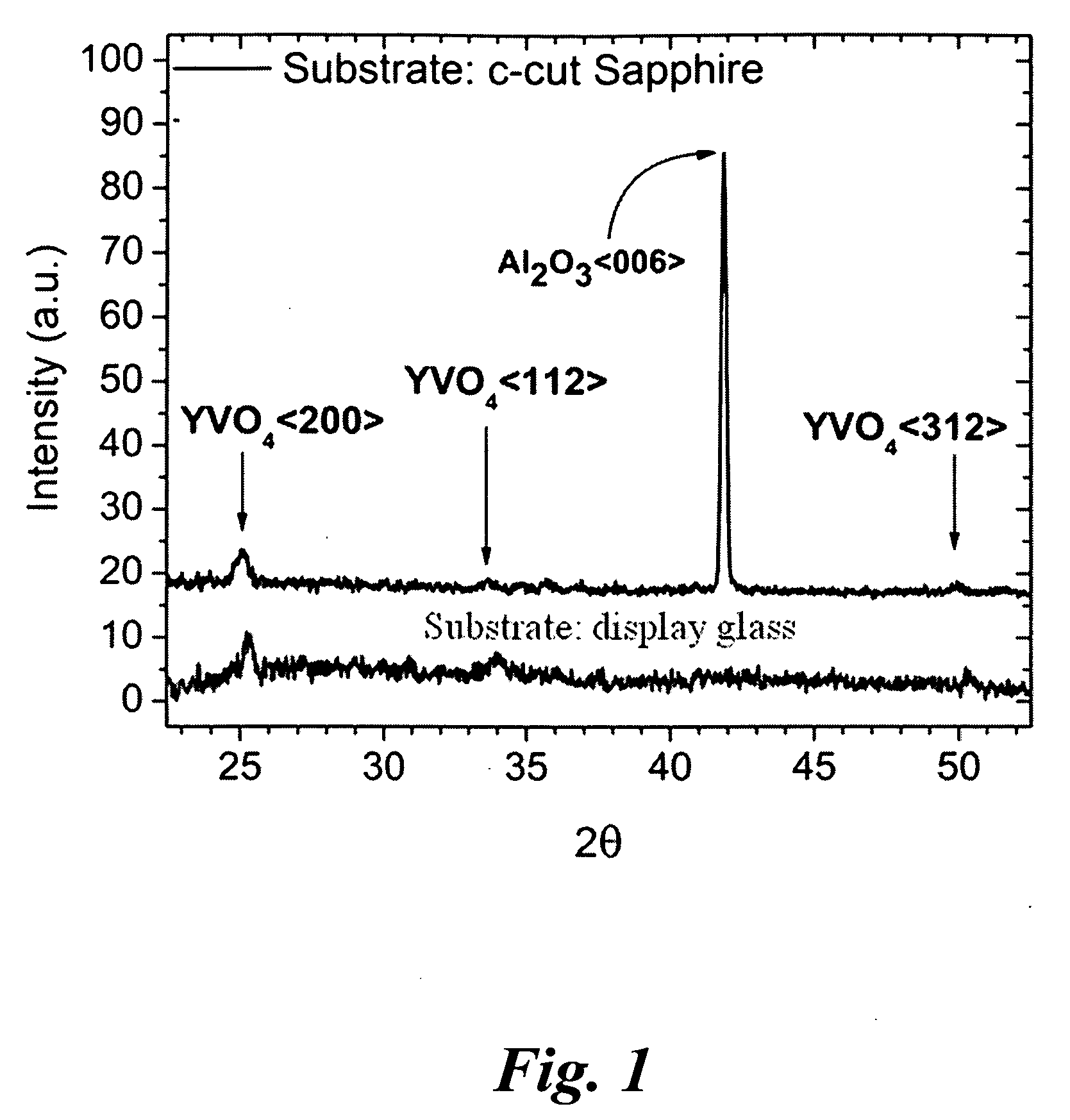
YVO4 films prepared with these methods suffer from lack of crystallographic orientation control and the incorporation of vanadium-poor or rich nonstoichiometric phases.
Preparation of thin film scintillators is a difficult process.

Method used


Image

  • Porous light-emitting compositions
  • Porous light-emitting compositions
  • Porous light-emitting compositions

Examples


example a

Solutions

[0049]A yttrium solution was prepared by mixing 1.3 g yttrium nitrate hexahydrate (99.9%, ALFA AESAR) with 1.0 g HEDTA (ALDRICH, 99.995% pure) and 1.0 g BASF polyethyleneimine polymer. The resulting solution was filtered through a 0.45 micron filter, diluted to 200 mL with nano pure water, and purified by Amicon filtration with a 3,000 MW cut-off filter. The final concentrated solution was 133 mM yttrium, determined by ICP / AES.

[0050]A europium solution was prepared by mixing 1.0 g of europium nitrate hexahydrate (99.9%, ACROS) with 1.0 g HEDTA (ALDRICH, 99.995% pure) and 1.0 g BASF polyethyleneimine polymer. The resulting solution was filtered through a 0.45 micron filter, diluted to 200 mL, and purified by Amicon filtration with a 3,000 MW cut-off filter. The final concentrated solution was 136 mM europium.

[0051]A vanadium solution was prepared by mixing 1.0 g vanadyl sulfate (ACROS) with 1.0 g HEDTA (ALDRICH, 99.995% pure) and 1.0 g BASF polyethyleneimine polymer. The res...

example b

[0058]P1-Photonic Crystals with one coat of YV / 5% Eu were prepared as follows. SiO2 crystals were coated with YV / 5% Eu using the PAD method of coating. Coating solutions were made by mixing calculated volumes of each solution to obtain a 1:1 mol ratio of Y to V. A calculated volume of Eu solution was added to the Y / V solution to obtain a 5% mol ratio of Eu. 283 mg of the solution was then dropped onto 32 mg of P1 photonic crystals in a 20-mL scintillation vial. The vial was rotated to ensure total coverage of the crystals by the coating solution. The coated crystals were then rotovapped under negative pressure in order to cause the solution to penetrate the cavities within the photonic crystals and remove excess water. When the crystals appeared dry, the crystals were transferred to a ceramic crucible. The crystals were then annealed in air with the following heating program: The temperature was ramped to 120° C. at 10° / min and held for 1 hour. The temperature was ramped to 450° C. ...

example c

[0059]P1-Photonic Crystals with two coats of YV / 5% Eu were prepared as follows. SiO2 crystals were coated with YV / 5% Eu using the PAD method of coating. Coating solutions were made by mixing calculated volumes of each solution to obtain a 1:1 mol ratio of Y to V. A calculated volume of Eu solution was added to the Y / V solution to obtain a 5% mol ratio of Eu. 194 mg of the solution was then dropped onto 32 mg of P1 photonic crystals in a 20-mL scintillation vial. The vial was rotated to ensure total coverage of the crystals by the coating solution. The coated crystals were then rotovapped under negative pressure in order to cause the solution to penetrate the cavities within the photonic crystals and remove excess water. When the crystals appeared dry, the crystals were transferred to a ceramic crucible. The crystals were then annealed in air with the following heating program: The temperature was ramped to 120° C. at 10° / min and held for 1 hour. The temperature was ramped to 450° C....


PUM

PropertyMeasurementUnit
pore sizesaaaaaaaaaa
extraction efficienciesaaaaaaaaaa

Abstract

Light-emitting devices are prepared by coating a porous substrate using a polymer-assisted deposition process. Solutions of metal precursor and soluble polymers having binding properties for metal precursor were coated onto porous substrates. The coated substrates were heated at high temperatures under a suitable atmosphere. The result was a substrate with a conformal coating that did not substantially block the pores of the substrate.

Description

RELATED APPLICATIONS[0001]This application claims the benefit of U.S. Provisional Application Ser. No. 61 / 063,154 entitled “Composite Phosphors Based on Coating Porous Substrates,” filed Jan. 30, 2008, and U.S. Provisional Application Ser. No. 61 / 063,153 entitled “Polymer-Assisted Deposition of Conformal Films on Porous Materials,” both hereby incorporated by reference.STATEMENT REGARDING FEDERAL RIGHTS[0002]This invention was made with government support under Contract No. DE-AC52-06NA25396 awarded by the U.S. Department of Energy. The government has certain rights in the invention.FIELD OF THE INVENTION[0003]The present new light-emitting devices that result from conformal films on porous materials, in particular luminescent metal oxide films, and more particularly these luminescent metal oxide films deposited on porous alumina and silica structures resulting in composite phosphors or scintillators.BACKGROUND OF THE INVENTION[0004]Phosphors find applications in many Light Emitting...

Claims


Application Information

Patent Timeline
Patent Type & Authority Applications(United States)
IPC IPC(8): B32B3/26C09K11/77C09K11/08B32B3/00
CPCC09K11/54C09K11/671H01L31/02322H01L31/055Y10T428/24149Y10T428/24496Y10T428/24942Y10T428/12479Y10T428/268Y10T428/249967Y10T428/249978Y10T428/249953Y10T428/249969Y10T428/24999Y10T428/24997
Inventor BURRELL, ANTHONY K.MCCLESKEY, THOMAS MARKJIA, QUANXIBAUER, EVEMUELLER, ALEXANDER H.
Owner TRIAD NAT SECURITY LLC
Why Eureka
Try Eureka