
Apparatus and Method for Reducing Noise In Fingerprint Sensing Circuits

a fingerprint sensing circuit and noise reduction technology, applied in the field of fingerprint sensing technology, can solve the problems of affecting the noise of each active capacitive sensor, and affecting the quality of the acquired fingerprint image, so as to reduce the amount of noise, and reduce the noise in the fingerprint sensing circuit

Active Publication Date: 2009-10-08
SYNAPTICS INC
View PDF100 Cites 102 Cited by
  • Summary
  • Abstract
  • Description
  • Claims
  • Application Information

AI Technical Summary

Benefits of technology

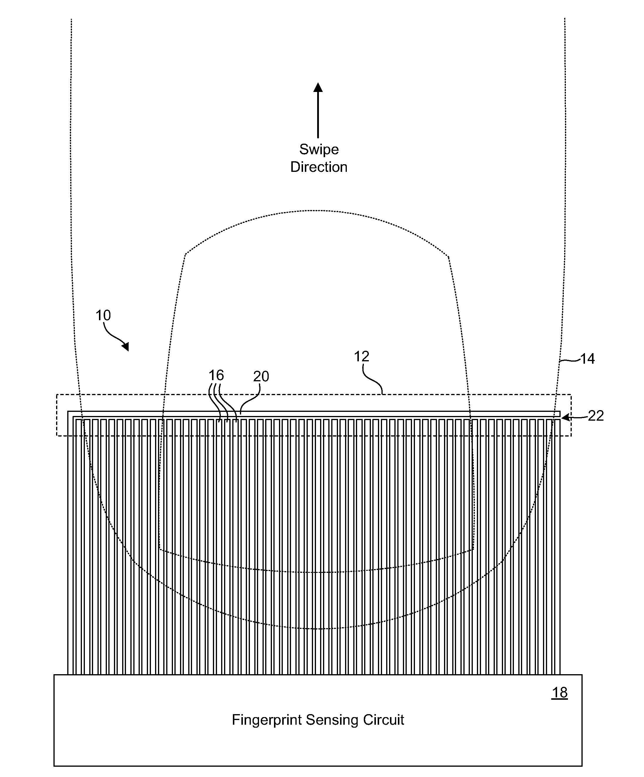
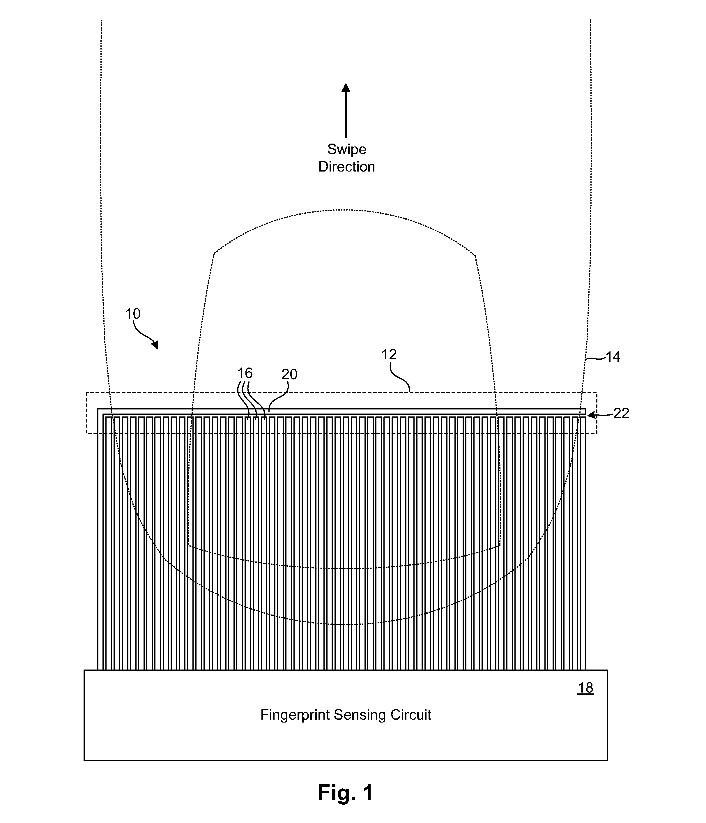
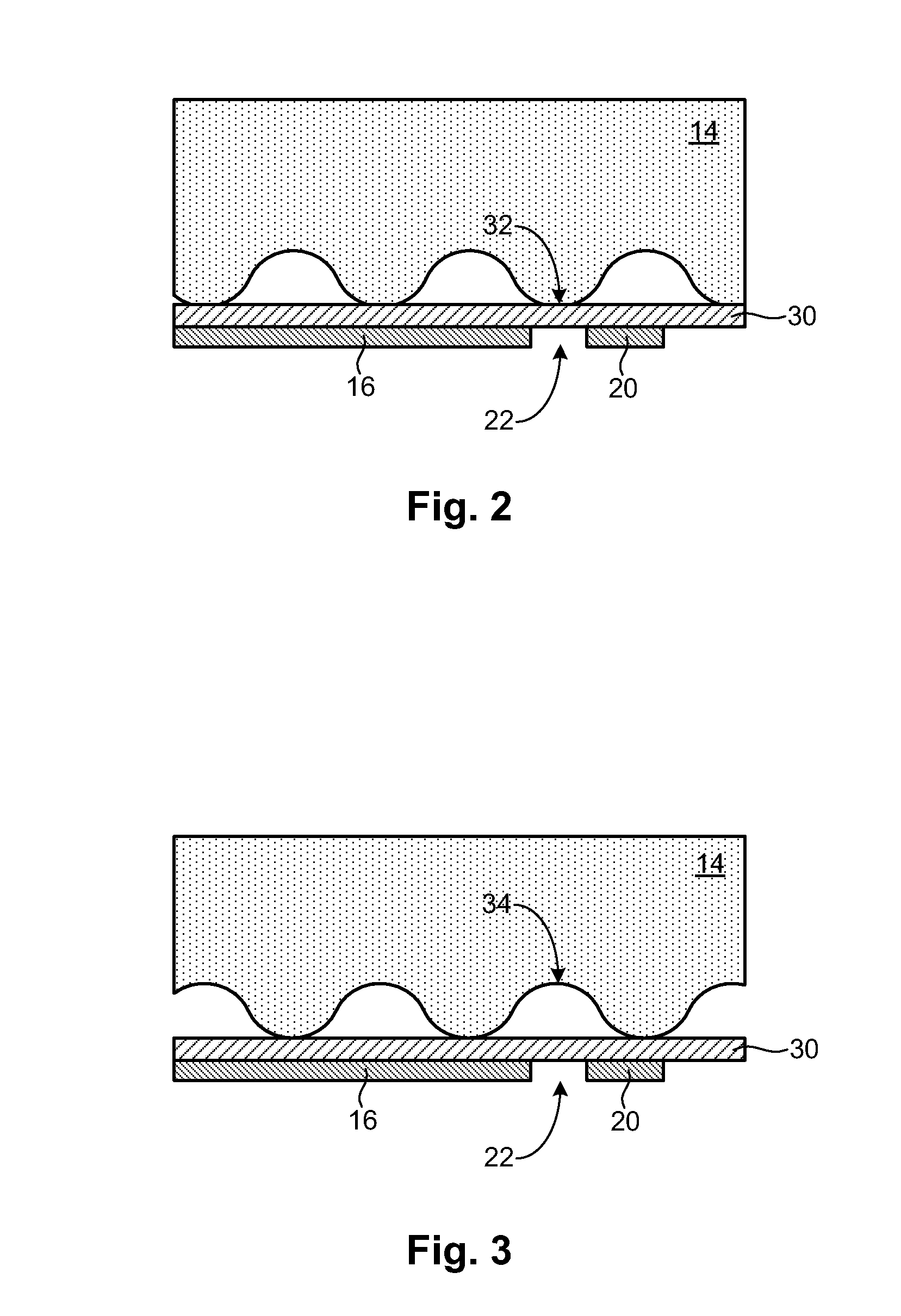
[0015]Consistent with the foregoing, an apparatus for reducing noise in fingerprint sensing circuits is disclosed in one embodiment of the invention as including a fingerprint sensing area onto which a user can apply a fingerprint. An analog front end is coupled to the fingerprint sensing area and is configured to generate an analog response signal. An analog-to-digital converter (ADC) samples the analog response signal and converts the sample to a digital value, which may be received by a digital device such as a processor or CPU. To reduce the amount of the noise that is present in the analog response signal and therefore reflected in the digital value, the digital device may be shut down while the ADC is sampling the analog response signal.
[0017]In another embodiment in accordance with the invention, a method for reducing noise in a fingerprint sensing circuit may include providing a fingerprint sensing area onto which a user can apply a fingerprint. An analog response signal associated with finger activity over the fingerprint sensing area may then be generated. The method may further include sampling the analog response signal and converting the sample to a digital value. This digital value may then be received by a digital device. To reduce the amount of noise that is present in the analog response signal during sampling and therefore reflected in the digital value, the method may further include shutting down the digital device while sampling the analog response signal.
[0018]In another embodiment in accordance with the invention, a method for reducing noise in fingerprint sensing circuits includes providing a fingerprint sensing area onto which a user can apply a fingerprint and generating an analog response signal in response to finger activity over the fingerprint sensing area. The analog response signal is then sampled and converted to a digital value. This digital value may then be received or processed by a CPU. To reduce the amount of the noise that is present in the analog response signal during sampling and reflected in the digital value, the method may further include turning off a clock signal to the CPU while sampling the analog response signal.

Problems solved by technology

Active capacitive sensors, however, may be adversely affected by dry or worn minutia, which may fail to drive the sensor's output amplifier.
Although each of the fingerprint sensing technologies described above may generate satisfactory fingerprint images, each may be adversely affected by noise, interference, and other effects.
For example, capacitive sensors may be particularly susceptible to noise and parasitic capacitive coupling, which may degrade the quality of the acquired fingerprint image.

Method used


Image

  • Apparatus and Method for Reducing Noise In Fingerprint Sensing Circuits
  • Apparatus and Method for Reducing Noise In Fingerprint Sensing Circuits
  • Apparatus and Method for Reducing Noise In Fingerprint Sensing Circuits

Examples


Embodiment Construction

[0014]The invention has been developed in response to the present state of the art, and in particular, in response to the problems and needs in the art that have not yet been fully solved by currently available fingerprint sensors. Accordingly, the invention has been developed to provide novel apparatus and methods for reducing noise in fingerprint sensing circuits. The features and advantages of the invention will become more fully apparent from the following description and appended claims and their equivalents, and also any subsequent claims or amendments presented, or may be learned by practice of the invention as set forth hereinafter.

[0015]Consistent with the foregoing, an apparatus for reducing noise in fingerprint sensing circuits is disclosed in one embodiment of the invention as including a fingerprint sensing area onto which a user can apply a fingerprint. An analog front end is coupled to the fingerprint sensing area and is configured to generate an analog response signa...


PUM


Abstract

An apparatus for reducing noise in fingerprint sensing circuits is disclosed in one embodiment of the invention as including a fingerprint sensing area onto which a user can apply a fingerprint. An analog front end is coupled to the fingerprint sensing area and is configured to generate an analog response signal. An analog-to-digital converter (ADC) samples the analog response signal and converts the sample to a digital value, which may be received by a digital device such as a processor or CPU. To reduce the amount of the noise that is present in the analog response signal and therefore reflected in the digital value, the digital device may be shut down while the ADC is sampling the analog response signal.

Description

BACKGROUND[0001]This invention relates to fingerprint sensing technology, and more particularly to apparatus and methods for reducing the effects of noise in fingerprint sensing circuits.[0002]Fingerprint sensing technology is increasingly recognized as a reliable, non-intrusive way to verify individual identity. Fingerprints, like various other biometric characteristics, are based on unalterable personal characteristics and thus are believed to be more reliable when identifying individuals. The potential applications for fingerprints sensors are myriad. For example, electronic fingerprint sensors may be used to provide access control in stationary applications, such as security checkpoints. Electronic fingerprint sensors may also be used to provide access control in portable applications, such as portable computers, personal data assistants (PDAs), cell phones, gaming devices, navigation devices, information appliances, data storage devices, and the like. Accordingly, some applicat...

Claims


Application Information

Patent Timeline
IPC IPC(8): G06K9/00G06V30/144
CPCG06K9/0002G06V40/1306
Inventor DEAN, GREGORY LEWISERHART, RICHARD ALEXANDERJANDU, JASWINDERTHOMPSON, ERIK JONATHON
Owner SYNAPTICS INC
Learn More