Electro-optical device, input device, and electronic apparatus

a technology of electrooptical devices and input devices, applied in the direction of optics, optical light guides, instruments, etc., can solve the problems of deteriorating display quality, unsatisfactory, and vulnerable external forces of liquid crystal display panels, so as to prevent the deterioration of color rendering properties of coloration layers and enhance the design quality of light-transmissive protection plates

Active Publication Date: 2009-10-15
JAPAN DISPLAY WEST
View PDF9 Cites 41 Cited by
  • Summary
  • Abstract
  • Description
  • Claims
  • Application Information

AI Technical Summary

Benefits of technology

[0011]An advantage of some aspects of the invention is to provide an electro-optical device that makes it possible to prevent the leakage of light from a liquid-crystal-display-panel side to a display side and further prevent the degradation of display quality while enhancing the design quality of a light-transmissive member by means of a coloration layer when the light-transmissive member on which the coloration layer is formed for improving design quality is used. The invention further provides, as an advantage of some aspects of the invention, an electronic apparatus that is provided with such an electro-optical device.

Problems solved by technology

A liquid crystal display panel is vulnerable to an external force such as a pressing force, a shock, and the like that is applied from the outside.
If a layer of air exists between the transparent protection cover and the liquid crystal display panel in such a configuration, light is diffused due to a difference in the index of refraction between these media, which results in degradation in display quality.
However, if such a light-color printed pattern is adopted, inner components provided at the liquid-crystal-display-panel side may be seen through when observed from the peripheral edge part of the transparent protection cover, which is not desirable.
In addition, it is difficult to make the air bubbles escape to the outside.
If any air bubble remains without being removed at the level-difference area part, there is a risk that display quality is adversely affected due to a difference in the index of refraction of the air bubble and the index of refraction of the light-transmissive adhesion sheet and the like.
Moreover, since a large level difference is formed on the transparent protection cover, a distance between the transparent protection cover and the liquid crystal display panel is also large.
Therefore, there is an adverse possibility that a stress is applied to the liquid crystal display panel in a direction of pulling the liquid crystal display panel toward the transparent protection cover due to the adhesion force of the light-transmissive adhesion sheet when the liquid crystal display panel and the transparent protection cover are bonded to each other with the use of the light-transmissive adhesion sheet.
In addition, there is an adverse possibility that a stress that causes the liquid crystal display panel to be deflected under the pulling force is applied to the liquid crystal display panel.
For this reason, display unevenness or other image problems might occur at the time of the driving of the liquid crystal display panel due to the deflection thereof, which results in degradation in display quality.
When light is irradiated from the touch-panel side toward the coloration layer, the color-rendering properties of the coloration layer deteriorate.
Because of the deterioration of the color-rendering properties of the coloration layer, the decoration layer looks bad, which is one problem of related art.

Method used


Image

  • Electro-optical device, input device, and electronic apparatus
  • Electro-optical device, input device, and electronic apparatus
  • Electro-optical device, input device, and electronic apparatus

Examples


second embodiment

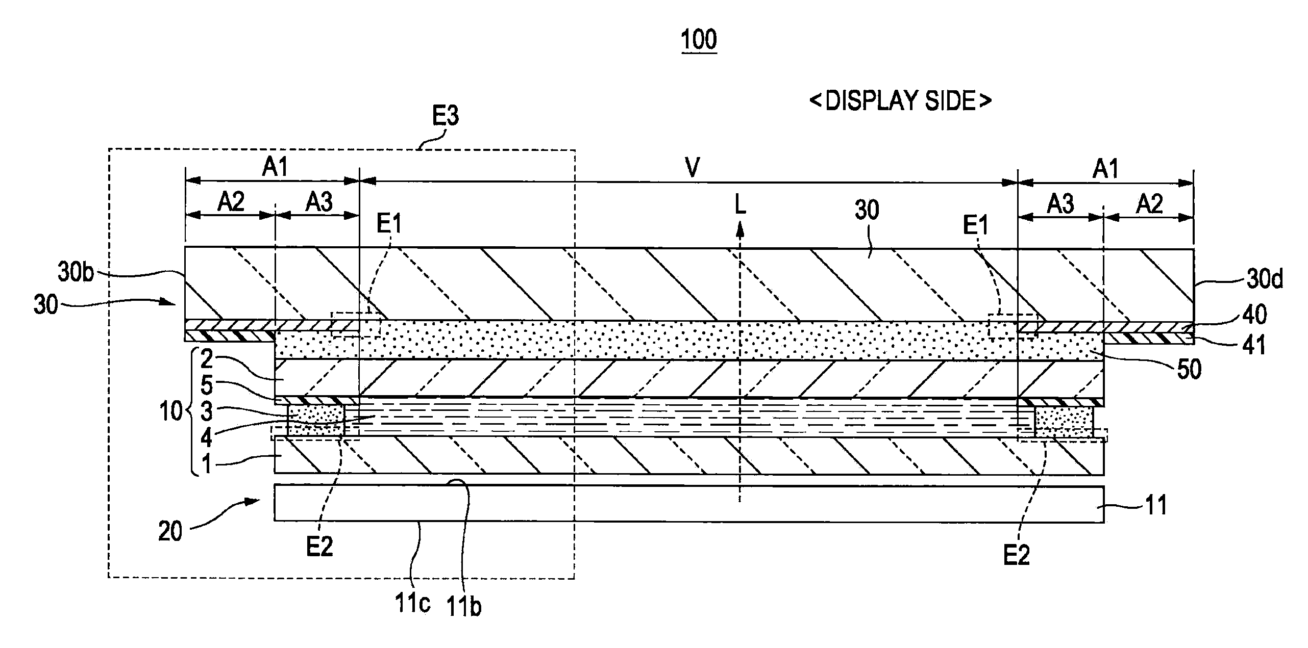
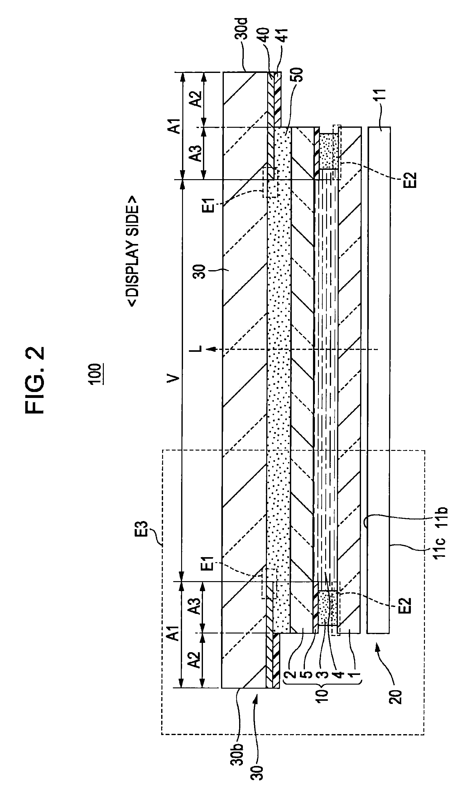
[0077]Next, with reference to FIG. 5, an explanation is given below of an exemplary configuration and other features of a liquid crystal device 100b according to a second embodiment of the invention. FIG. 5 is a sectional view that schematically illustrates an example of the layer structure of the liquid crystal device 100b according to the second embodiment of the invention, which is taken along a section line corresponding to that of the liquid crystal device 100 explained earlier while referring to FIG. 2.

[0078]The configuration of the liquid crystal device 100b according to the second embodiment of the invention differs from that of the liquid crystal device 100 according to the first embodiment of the invention in terms of the structures of its liquid crystal display panel and illumination device. Except for these differences, the structure of the liquid crystal device 100b according to the second embodiment of the invention is the same as that of the liquid crystal device 100 ...

third embodiment

[0089]Next, with reference to FIG. 7, an explanation is given below of an exemplary configuration and other features of a liquid crystal device 100d according to a third embodiment of the invention. Therefore, in the following description of the liquid crystal device 100d according to the third embodiment of the invention, the same reference numerals are consistently used for the same components as those of the liquid crystal device 100 according to the first embodiment of the invention and the liquid crystal device 100b according to the second embodiment of the invention so as to omit, if appropriate, any redundant explanation or simplify explanation thereof. FIG. 7 is a sectional view that schematically illustrates an example of the layer structure of the liquid crystal device 100d according to the third embodiment of the invention, which is taken along a section line corresponding to that of the liquid crystal device 100 explained earlier while referring to FIG. 2.

[0090]In the co...

modification examples

OTHER MODIFICATION EXAMPLES

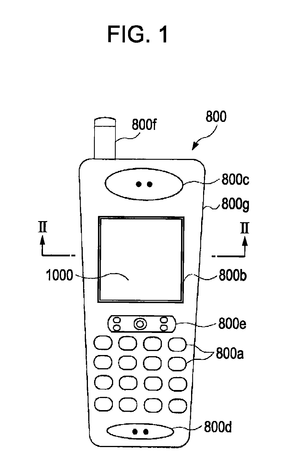
[0094]Next, with reference to FIG. 8A, another modification example of an exemplary embodiment of the invention is explained below. FIG. 8A is an enlarged sectional view that schematically illustrates an example of the essential components of a liquid crystal device 100e according to another modification example of an exemplary embodiment of the invention; specifically, FIG. 8A shows a partial section that corresponds to a section area E3 shown by a dotted line in FIG. 2. FIG. 8A further illustrates a partial section of the case (frame) 800g that supports the peripheral edge part of the light-transmissive protection plate 30.

[0095]The case 800g of the mobile phone 800 has a dent 800ga that is formed as an area part that supports the peripheral edge part of the light-transmissive protection plate 30. The peripheral edge part of the light-transmissive protection plate 30 is fitted in the dent 800ga of the case 800g so that the case 800g supports the liquid c...


PUM

PropertyMeasurementUnit
areaaaaaaaaaaa
electro-opticalaaaaaaaaaa
external forceaaaaaaaaaa

Abstract

An electro-optical device includes: an electro-optical panel; a light-transmissive member that overlaps the electro-optical panel and has a protruding part that protrudes so as to be positioned outside an edge of the electro-optical panel, the light-transmissive member having a first area and a second area that is located outside the first area; a coloration layer that is formed on a surface of the light-transmissive member at the second area; an adhesive material that is provided between a part of the coloration layer and a corresponding part of the electro-optical panel as well as between the part of the light-transmissive member and a corresponding part of the electro-optical panel; and a first light-shielding layer formed over one surface of the light-transmissive member, and the first light-shielding layer being formed at an area where the coloration layer does not overlap the adhesive material in a plan view.

Description

BACKGROUND[0001]1. Technical Field[0002]The present invention relates to the structure of an electro-optical device that includes an electro-optical panel and a light-transmissive member that overlaps the electro-optical panel when viewed in plan, though not limited thereto.[0003]2. Related Art[0004]An electro-optical device is used in a variety of electronic apparatuses such as a mobile phone, a personal digital assistance, and the like for the purpose of displaying video information such as images.[0005]An example of such an electro-optical device is a liquid crystal display device that is provided with a liquid crystal display panel, which is made up of a pair of substrates and liquid crystal that is sandwiched and sealed between the pair of substrates. A liquid crystal display panel is vulnerable to an external force such as a pressing force, a shock, and the like that is applied from the outside. In order to protect a weak liquid crystal display panel against an external force,...

Claims


Application Information

Patent Timeline
Patent Type & Authority Applications(United States)
IPC IPC(8): G02F1/1333
CPCG02F1/133308G02F2201/50G02F2001/13332G02F1/133512G02F1/13332
Inventor SAKURAI, SHINJI
Owner JAPAN DISPLAY WEST
Why Eureka
Try Eureka