Display device with touch panel
a display device and touch panel technology, applied in non-linear optics, instruments, optics, etc., can solve the problems of deterioration of optical characteristics and reduction of characteristics of display devices incorporating touch panels, and achieve the effect of suppressing the reduction of characteristics of display devices
- Summary
- Abstract
- Description
- Claims
- Application Information
AI Technical Summary
Benefits of technology
Problems solved by technology
Method used
Image

Examples
first embodiment
[0032]A first embodiment of the present invention is described by way of example in which the present invention is applied to a display device with a touch panel, which includes the touch panel on a display panel such as a liquid crystal display panel.
[0033]FIGS. 1 to 5 illustrate the display device with the touch panel according to the first embodiment of the present invention:
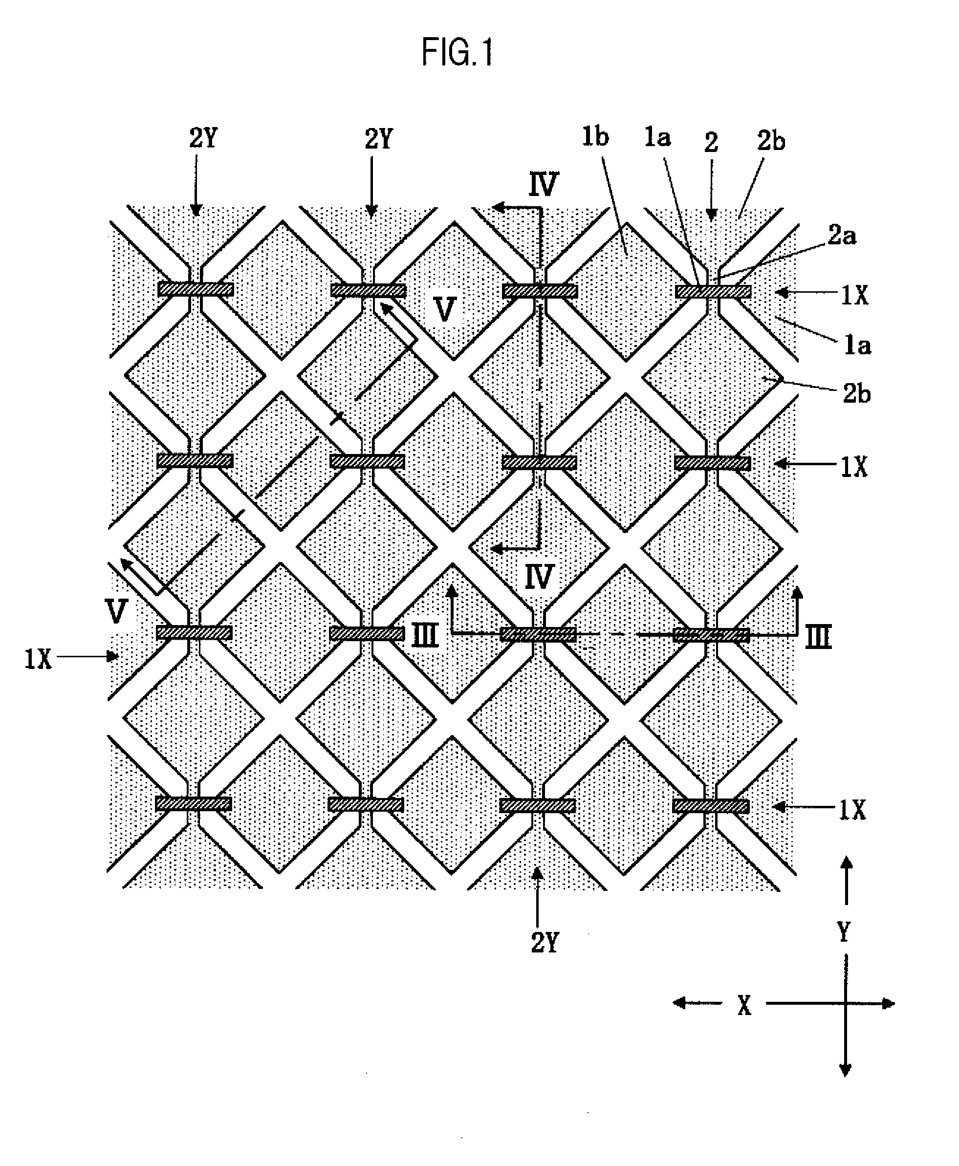
[0034]FIG. 1 is a plan diagram illustrating electrode patterns of a touch panel incorporated in the display device with the touch panel;
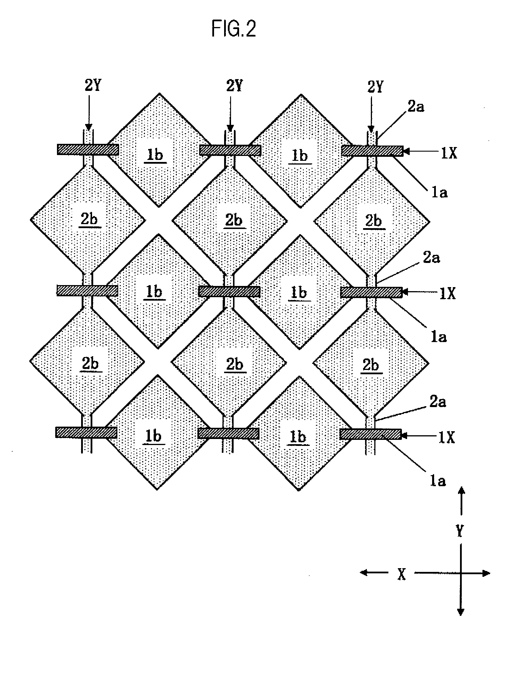
[0035]FIG. 2 is an enlarged plan diagram of a part of FIG. 1;
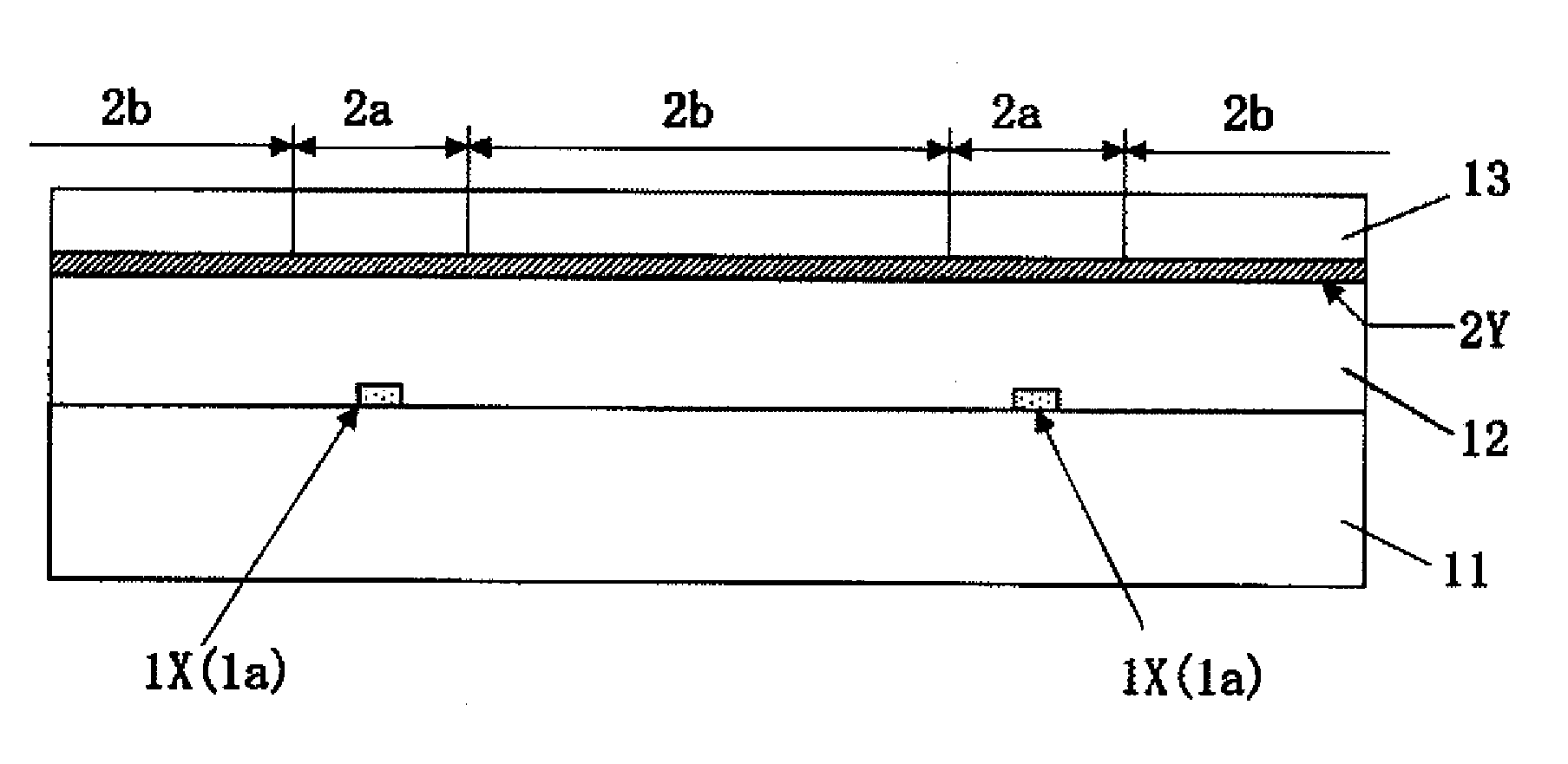
[0036]FIG. 3 is a sectional diagram illustrating a sectional structure cut on the line III-III of FIG. 1;
[0037]FIG. 4 is a sectional diagram illustrating a sectional structure cut on the line IV-IV of FIG. 1; and
[0038]FIG. 5 is a block diagram illustrating a schematic configuration of the display device with the touch panel.
[0039]In FIG. 5, a touch panel 20 illustrates a sectional structure cut on the line V-V of FI...
second embodiment
[0064]FIGS. 6 to 8 illustrate a display device with a touch panel according to a second embodiment of the present invention:
[0065]FIG. 6 is a plan diagram illustrating electrode patterns of a touch panel incorporated in the display device with the touch panel;
[0066]FIG. 7 is a sectional diagram illustrating a sectional structure cut on the line VII-VII of FIG. 6; and
[0067]FIG. 8 is a sectional diagram illustrating a sectional structure cut on the line VIII-VIII of FIG. 6.
[0068]The display device with the touch panel of the second embodiment is basically similar in configuration to that of the first embodiment, and is different as follows.
[0069]In the first embodiment, as illustrated in FIGS. 1 to 4, the electrode 2Y and the second portion 1b of the electrode 1X are formed on the lower conductive layer, and the first portion 1a of the electrode 1X is formed on the upper conductive layer. In the second embodiment, however, as illustrated in FIGS. 6 to 8, a first portion 1a of an elect...
PUM
 Abstract
Description
Claims
Application Information
 - Generate Ideas
- Intellectual Property
- Life Sciences
- Materials
- Tech Scout
- Unparalleled Data Quality
- Higher Quality Content
- 60% Fewer Hallucinations
Browse by: Latest US Patents, China's latest patents, Technical Efficacy Thesaurus, Application Domain, Technology Topic, Popular Technical Reports.
© 2025 PatSnap. All rights reserved.Legal|Privacy policy|Modern Slavery Act Transparency Statement|Sitemap|About US| Contact US: help@patsnap.com