Field effect transistor

Active Publication Date: 2011-12-22
SEMICON ENERGY LAB CO LTD
View PDF20 Cites 71 Cited by
  • Summary
  • Abstract
  • Description
  • Claims
  • Application Information

AI Technical Summary

Benefits of technology

[0065]In a normal MISFET, a trap level or the like is generated at an interface between a gate insulating film and a semiconductor to reduce FET characteristics; however, the influence of the interface can be reduced with a structure in which carriers flow in a portion that

Problems solved by technology

However, oxygen deficiency is likely to be caused in indium oxide or an oxide semiconductor including indi

Method used


Image

  • Field effect transistor
  • Field effect transistor
  • Field effect transistor

Examples


embodiment 1

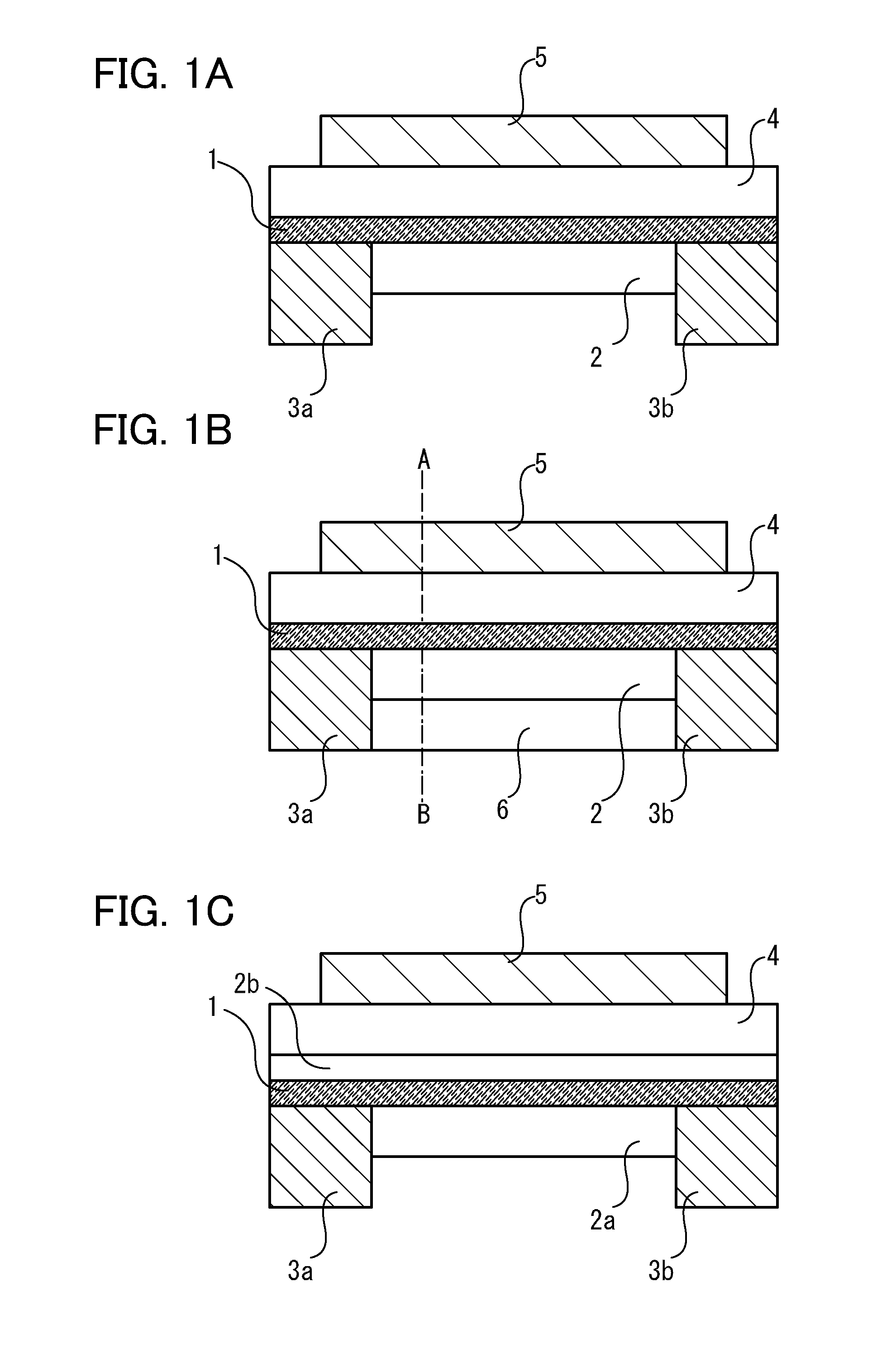
[0077]In this embodiment, a manufacturing method of a FET will be described with reference to FIGS. 4A to 4F. First, as illustrated in FIG. 4A, a conductive layer 102 is formed over a substrate 101. A variety of substrates can be given as examples of the substrate 101, but the substrate 101 needs to have such a property as to withstand the subsequent treatment. Further, it is preferable that a surface of the substrate 101 have an insulating property. Accordingly, the substrate 101 is preferably an insulator alone; an insulator, metal, or semiconductor whose surface is provided with an insulating layer; or the like.

[0078]As the insulator, various kinds of glasses, sapphire, quartz, ceramics, plastics, or the like can be used. As the metal, aluminum, copper, stainless steel, silver, or the like can be used. As the semiconductor, silicon, germanium, silicon carbide, gallium nitride, or the like can be used. In this embodiment, barium borosilicate glass is used as the substrate 101.

[007...

embodiment 2

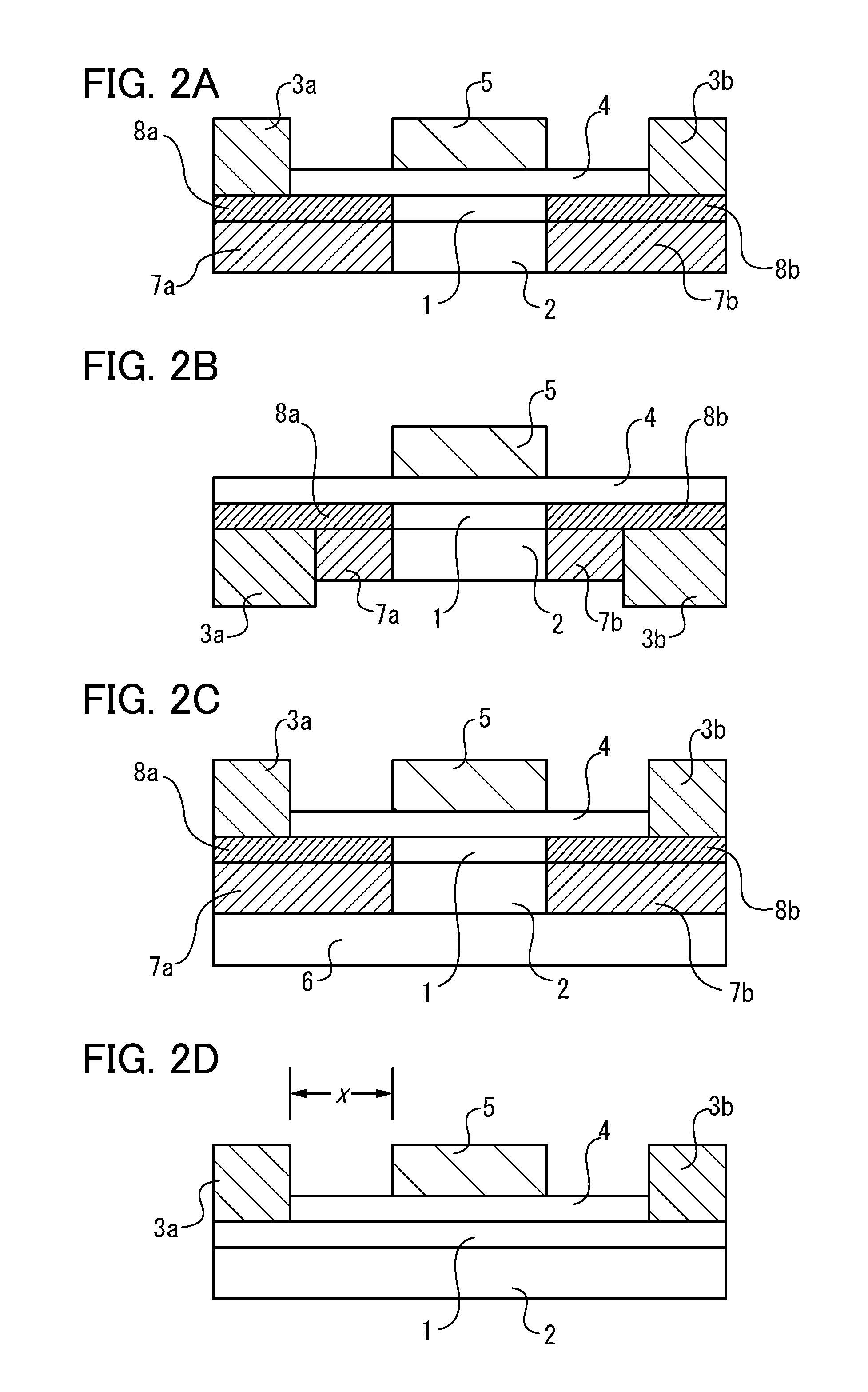
[0092]In this embodiment, a manufacturing method of a FET will be described with reference to FIGS. 5A to 5E. As illustrated in FIG. 5A, a conductive film 202, an insulating film 203, a first oxide semiconductor film 204, a second oxide semiconductor film 205, and an oxide insulating film 206 are stacked over a substrate 201. Formation of these films is preferably performed successively without exposure to the air on the way in order to keep interfaces of the films clean. In addition, successive film formation is also effective in order to make the hydrogen concentration in the multi-layer films lower than or equal to 1×10¹⁸ atoms / cm3, preferably lower than or equal to 1×10¹⁶ atoms / cm3.

[0093]The substrate 201, the conductive film 202, the insulating film 203, the first oxide semiconductor film 204, the second oxide semiconductor film 205, and the oxide insulating film 206 may be formed using materials, thicknesses, and formation methods that are described in Embodiment 1 as being su...

embodiment 3

[0122]In this embodiment, a manufacturing method of a FET will be described with reference to FIGS. 6A to 6D. As illustrated in FIG. 6A, an oxide insulating film 302, a second oxide semiconductor film 303, a first oxide semiconductor film 304, and an insulating film 305 are stacked over a substrate 301. Formation of theses films is preferably performed successively without exposure to the air on the way in order to keep interfaces of the films clean.

[0123]For example, a silicon wafer may be used as the substrate 301, a 200-nm-thick silicon oxide film may be used as the oxide insulating film 302, a 50-nm-thick gallium oxide film may be used as the second oxide semiconductor film 303, a 1-nm-thick indium oxide film may be used as the first oxide semiconductor film 304, and a 2-nm-thick silicon oxide film may be used as the insulating film 305. The oxide insulating film 302 may be formed by performing thermal oxidation on the substrate 301. The second oxide semiconductor film 303, the ...


PUM


Abstract

An insulating film is provided over one surface of a first semiconductor layer including a first oxide semiconductor including indium as a main component, and a second semiconductor layer including an i-type second oxide semiconductor is provided in contact with the other surface. The energy difference between a vacuum level and a Fermi level in the second oxide semiconductor is larger than that in the first oxide semiconductor. In the first semiconductor layer, a region in the vicinity of the junction surface with the second oxide semiconductor which satisfies the above condition is a region having an extremely low carrier concentration (a quasi-i-type region). By using the region as a channel, the off-state current can be reduced. Further, a drain current of the FET flows through the first oxide semiconductor having a high mobility; accordingly, a large amount of current can be extracted.

Description

TECHNICAL FIELD[0001]The present invention relates to a field effect transistor (FET) including an oxide semiconductor.BACKGROUND ART[0002]A field effect transistor (FET) is a device in which regions called a source and a drain are provided in a semiconductor, each of the regions is provided with an electrode, potentials are supplied to the electrodes, and an electric field is applied to the semiconductor with the use of an electrode called a gate through an insulating film or a Schottky barrier so that the state of the semiconductor is controlled, whereby current flowing between the source and the drain is controlled. As the semiconductor, Group IV elements (also referred to as Group 14 elements) such as silicon and germanium, Group III-V compounds such as gallium arsenide, indium phosphide, and gallium nitride, Group II-VI compounds such as zinc sulfide and cadmium telluride, and the like can be given.[0003]In recent years, FETs in which oxides such as indium oxide (Patent Documen...

Claims


Application Information

Patent Timeline
IPC IPC(8): H01L29/78
CPCH01L29/7869H01L21/02565H01L21/823814H01L29/41725H01L29/78696H01L29/06H01L29/78H01L29/786H01L29/78693H01L29/24H01L29/66969
Inventor TAKEMURA, YASUHIKO
Owner SEMICON ENERGY LAB CO LTD
Why Eureka
Try Eureka