Non-volatile semiconductor storage device and method of manufacturing the same

a non-volatile, semiconductor technology, applied in the direction of semiconductor devices, basic electric elements, electrical appliances, etc., can solve the problems of difficult to achieve such refinement, and inability to meet the requirements of euv exposure devices. , to achieve the limit of physical improvement, such as the breakdown voltage between devices, the effect of achieving the limi

Active Publication Date: 2009-10-29
KIOXIA CORP
View PDF8 Cites 294 Cited by
  • Summary
  • Abstract
  • Description
  • Claims
  • Application Information

AI Technical Summary

Benefits of technology

[0010]One aspect of the present invention provides a non-volatile semiconductor storage device comprising: a first layer functioning as a plurality of electrically rewritable memory cells connected in series; and a second layer provided on the periphery of the first layer, the first layer comprising: a plurality of first conductive layers extending parallel to a substrate and laminated in a direction perpendicular to the substrate, the first conductive layers functioning as control gates of the memory cells, a first insulation layer formed on an upper layer of the plurality of first conductive layers; a first semiconductor layer formed to penetrate the plurality of first conductive layers; and a charge accumulation layer formed between the first conductive layers and the first semiconductor layer and configured to be able to accumulate charges, respective ends of the first conductive layers being formed in a stepwise manner in relation to each other in a first direction, the second layer comprising: a plurality of second conductive layers extending in parallel to the substrate and laminated in a direction perpendicular to the substrate, the second conductive layers being formed in the same layer as the plurality of first conductive layers; and a second insulation layer formed on an upper layer of the plurality of second conductive layers, and respective ends of the second conductive layers being formed to align along a straight line extending in a direction substantially perpendicular to the substrate at a predetermined area.

Problems solved by technology

Although some measures are taken to reduce the dimension for each device (refinement) to increase memory storage capacity, recent years are facing challenges in such refinement from the viewpoint of cost and technology.
However, in currently available ArF immersion lithography technology, for example, the resolution limit has been reached around the 40 nm design rule and so EUV exposure devices have to be introduced for further refinement.
However, the EUV exposure devices are expensive and infeasible in view of the costs.
In addition, if such refinement is accomplished, it is assumed that physical improvement limit, such as in breakdown voltage between devices, would be reached unless driving voltage can be scaled, for example.
Thus, it is likely that difficulties would be encountered in device operation itself.

Method used


Image

  • Non-volatile semiconductor storage device and method of manufacturing the same
  • Non-volatile semiconductor storage device and method of manufacturing the same
  • Non-volatile semiconductor storage device and method of manufacturing the same

Examples


first embodiment

Configuration of Non-Volatile Semiconductor Storage Device 100 in First Embodiment

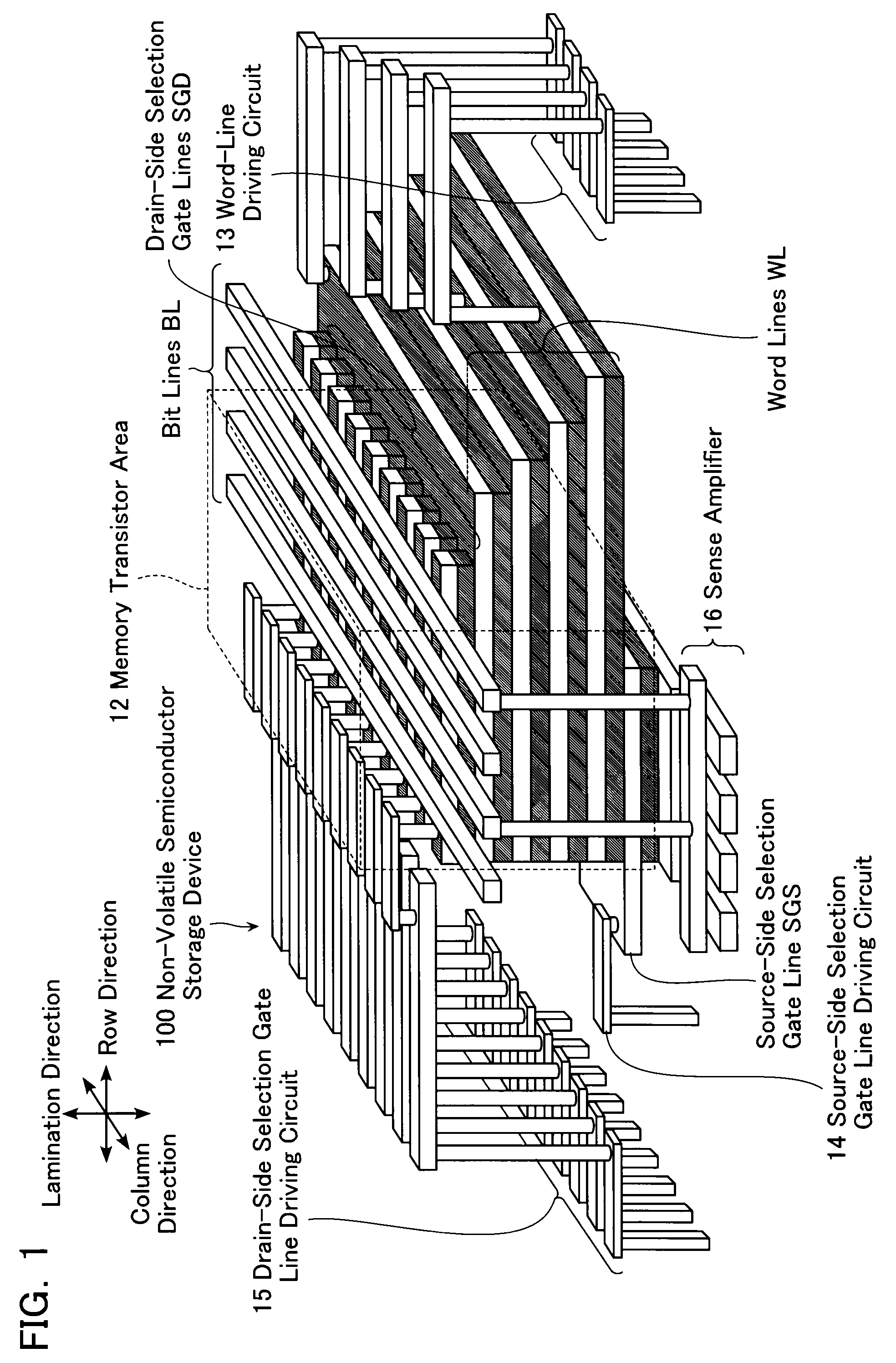
[0046]FIG. 1 schematically illustrates a non-volatile semiconductor storage device 100 according to a first embodiment of the present invention. As illustrated in FIG. 1, the non-volatile semiconductor storage device 100 according to the first embodiment mainly comprises: a memory transistor area (first area) 12; a word-line driving circuit 13; a source-side selection gate line (SGS) driving circuit 14; a drain-side selection gate line (SGD) driving circuit 15; and a sense amplifier 16. The memory transistor area 12 has memory transistors for storing data. The word-line driving circuit 13 controls voltage applied to word lines WL. The source-side selection gate line (SGS) driving circuit 14 controls voltage applied to the source-side selection gate line SGS. The drain-side selection gate line (SGD) driving circuit 15 controls voltage applied to drain-side selection gate lines (SGD). The sense amplifier...

second embodiment

Specific Configuration of Non-Volatile Semiconductor Storage Device 100a in Second Embodiment

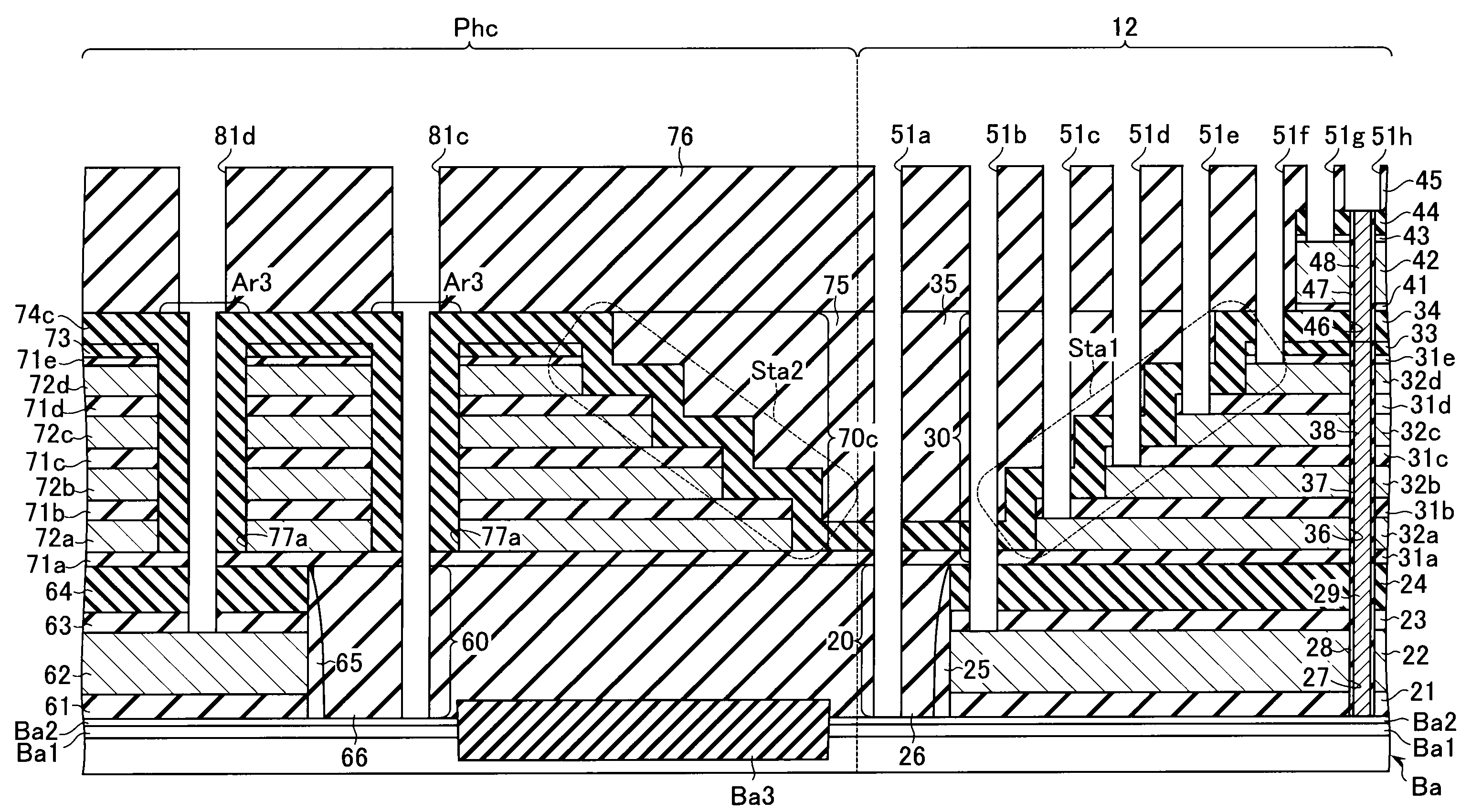
[0130]Referring now to FIG. 18, a specific configuration of a non-volatile semiconductor storage device 100a according to a second embodiment will be described below. FIG. 18 is a cross-sectional view in the row direction of the non-volatile semiconductor storage device 100a according to the second embodiment. Note that the same reference numerals represent the same components as the first embodiment and description thereof will be omitted in the second embodiment.

[0131]As illustrated in FIG. 18, the non-volatile semiconductor storage device 100a has a peripheral area Pha different from the first embodiment. The peripheral area Pha has a second CMP dummy layer 70a different from the first embodiment.

[0132]The second CMP dummy layer 70a has a dummy memory protection insulation layer 74a different from the first embodiment. Unlike the first embodiment, the dummy memory protection insulation la...

third embodiment

Specific Configuration of Non-Volatile Semiconductor Storage Device 100b in Third Embodiment

[0145]Referring now to FIG. 25, a specific configuration of a non-volatile semiconductor storage device 100b according to a third embodiment will be described below. FIG. 25 is a cross-sectional view in the row direction of the non-volatile semiconductor storage device 100b according to the third embodiment. Note that the same reference numerals represent the same components as the first and second embodiments and description thereof will be omitted in the third embodiment.

[0146]As illustrated in FIG. 25, the non-volatile semiconductor storage device 100b has a peripheral area Phb different from the first and second embodiments. The peripheral area Phb has a second CMP dummy layer 70b different from the first and second embodiments.

[0147]The second CMP dummy layer 70b has a dummy memory protection insulation layer 74b different from the first and second embodiments. Unlike the first and secon...


PUM


Abstract

A non-volatile semiconductor storage device includes a first layer and a second layer. The first layer includes: a plurality of first conductive layers extending in parallel to a substrate and laminated in a direction perpendicular to the substrate; a first insulation layer formed on an upper layer of the plurality of first conductive layers; a first semiconductor layer formed to penetrate the plurality of first conductive layers; and a charge accumulation layer formed between the first conductive layers and the first semiconductor layer. Respective ends of the first conductive layers are formed in a stepwise manner in relation to each other in a first direction. The second layer includes: a plurality of second conductive layers extending in parallel to the substrate and laminated in a direction perpendicular to the substrate, the second conductive layers being formed in the same layer as the plurality of first conductive layers; and a second insulation layer formed on an upper layer of the plurality of second conductive layers. Respective ends of the second conductive layers are formed to align along a straight line extending in a direction substantially perpendicular to the substrate at a predetermined area.

Description

CROSS-REFERENCE TO RELATED APPLICATIONS[0001]This application is based upon and claims the benefit of priority from the prior Japanese Patent Application No. 2008-117508, filed on Apr. 28, 2008, the entire contents of which are incorporated herein by reference.BACKGROUND OF THE INVENTION[0002]1. Field of the Invention[0003]The present invention relates to an electrically rewritable non-volatile semiconductor storage device and a method of manufacturing the same.[0004]2. Description of the Related Art[0005]Conventionally, LSIs are formed by integration of devices in a two-dimensional plane on the silicon substrate. Although some measures are taken to reduce the dimension for each device (refinement) to increase memory storage capacity, recent years are facing challenges in such refinement from the viewpoint of cost and technology. Such refinement requires further improvements in photolithography technology. However, in currently available ArF immersion lithography technology, for exa...

Claims


Application Information

Patent Timeline
Patent Type & Authority Applications(United States)
IPC IPC(8): H01L29/78H01L21/28
CPCH01L27/105H01L27/115H01L27/11582H01L27/11578H01L27/11573H10B69/00H10B43/20H10B43/40H10B43/27
Inventor TANAKA, HIROYASUKATSUMATA, RYOTAKITO, MASARUFUKUZUMI, YOSHIAKIKIDOH, MASARUKOMORI, YOSUKEAOCHI, HIDEAKIISHIDUKI, MEGUMIMATSUOKA, YASUYUKI
Owner KIOXIA CORP
Why Eureka
Try Eureka