Interconnect substrate and electronic circuit mounted structure

a technology of interconnect substrates and electronic circuits, applied in the direction of electrical apparatus construction details, electrical apparatus details, cross-talk/noise/interference reduction, etc., can solve the problems of reduced soldering area, reduced bonding strength, and failure to connect mobile devices

Inactive Publication Date: 2009-10-29
PANASONIC CORP
View PDF3 Cites 32 Cited by
  • Summary
  • Abstract
  • Description
  • Claims
  • Application Information

AI Technical Summary

Problems solved by technology

This results in reduced soldering area, which in turn causes reduced bonding strength.
This leads to connection failures in mobile devices, which are often subject to impact, causing loss of reliability.
However, if the circuit boards re connected with the aforementioned conventional interconnect substrate, and adhesive resin is applied on their outer side face, the adhesive resin may splatter or a connection failure may occur between the circuit boards and interconnect substrate due to thermal expansion of the air in the space enclosed by the two circuit boards and interconnect substrate on heating the structure to cure the adhesive resin.
This may ultimately result in a connection failure between the circuit boards and interconnect substrate, causing loss of reliability.
If the viscosity of

Method used


Image

  • Interconnect substrate and electronic circuit mounted structure
  • Interconnect substrate and electronic circuit mounted structure
  • Interconnect substrate and electronic circuit mounted structure

Examples


first exemplary embodiment

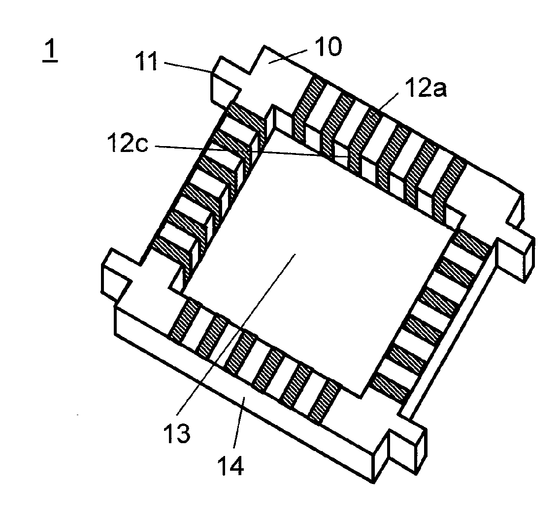
[0054]FIGS. 1A to 1D illustrate an interconnect substrate in the first exemplary embodiment of the present invention. FIG. 1A is a schematic perspective view, FIG. 1B is a schematic plan view, FIG. 1C is a sectional view taken along line IC-IC in FIG. 1B, and FIG. 1D is a sectional view taken along line 1D-1D in FIG. 1B.

[0055]Interconnect substrate 1 in this exemplary embodiment has a frame-like polygonal shape, and includes housing 10 with protrusion 11 provided on its outer side face, and a plurality of connecting terminal electrodes 12 connecting top and bottom faces of housing 10. In this exemplary embodiment, two protrusions 11 are provided on each of two opposing outer side faces of housing 10. These protrusions 11 have the same thickness as that of housing 10, as shown in the drawings. Inside housing 10 is opening 13.

[0056]Housing 10 with protrusions 11 can be easily formed by processing resin, such as liquid crystal polymer, polyphenylene sulfide, or polyethylene terephthala...

second exemplary embodiment

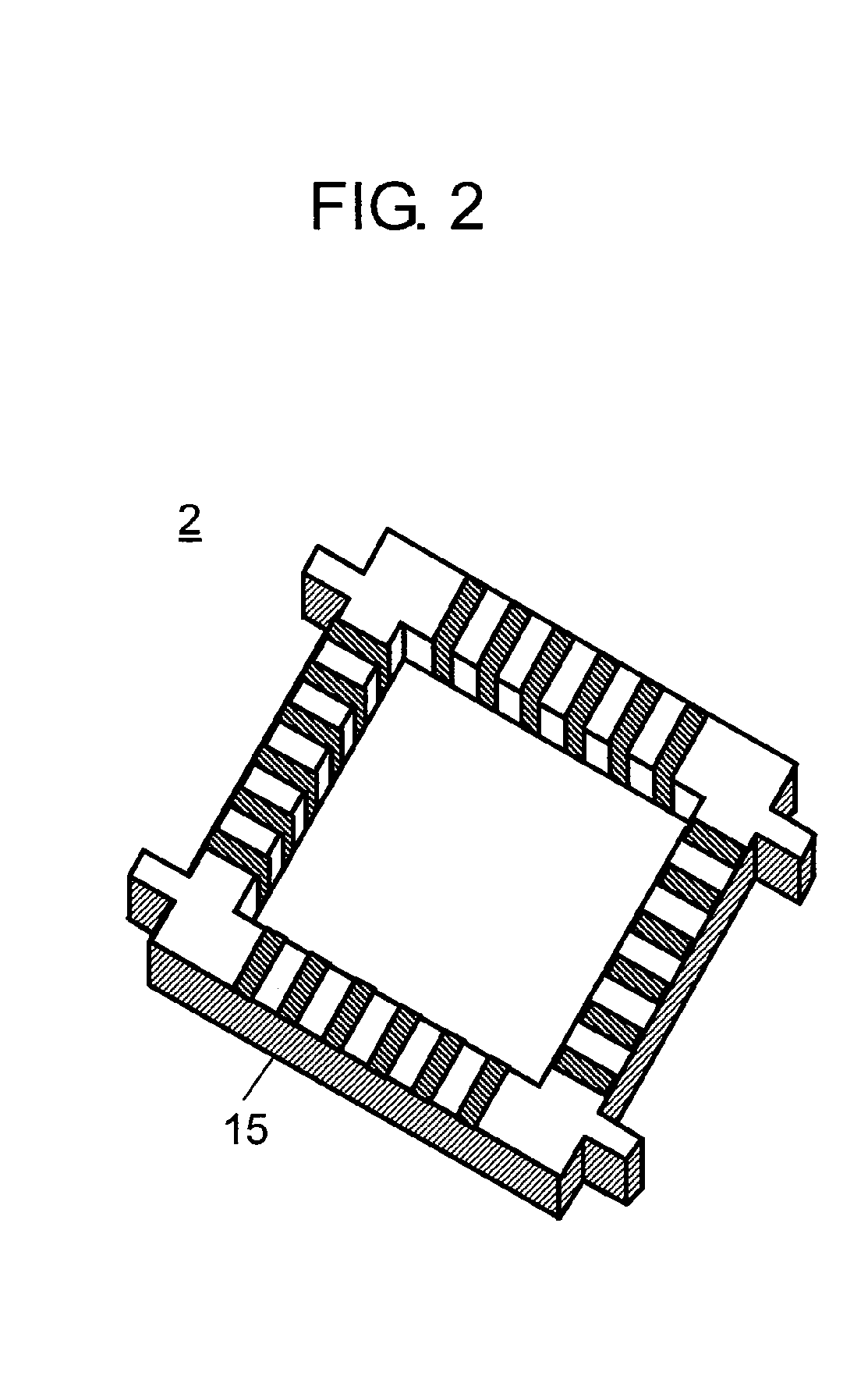
[0087]FIGS. 5A to 5C show an interconnect substrate in the second exemplary embodiment of the present invention. FIG. 5A is a schematic perspective view, FIG. 5B is a schematic plan view, and FIG. 5C is a sectional view taken along line 5C-5C in FIG. 5B.

[0088]Compared to interconnect substrate 1 in the first exemplary embodiment, interconnect substrate 3 in this exemplary embodiment has at least two protrusions 21 on each of four outer side faces of housing 20.

[0089]These protrusions 21 have the thickness same as the thickness of housing 20, as shown in the drawings. Inside housing 20 is opening 23. Connecting terminal electrode 22 can be formed by etching a predetermined pattern after plating copper on the top face, inner side face, and bottom face of housing 20 typically by using both electroless plating and electrolytic plating, same as that in the first exemplary embodiment. This achieves integral connection of top face terminal electrode 22a provided on the top face and bottom ...

third exemplary embodiment

[0112]FIGS. 8A to 8C show an interconnect substrate in the third exemplary embodiment of the present invention. FIG. 8A is a schematic perspective view, FIG. 8B is a schematic plan view, and FIG. 8C is a sectional view taken along line 8C-8C in FIG. 8B.

[0113]FIGS. 9A and 9B show electronic circuit mounted structure 300 using interconnect substrate 6 in this exemplary embodiment. FIG. 9A is a schematic sectional view, and FIG. 9B is a magnified sectional view of portion G in FIG. 9A.

[0114]Compared to interconnect substrate 1 in the first exemplary embodiment, interconnect substrate 6 in this exemplary embodiment has top face terminal electrode 32a and bottom face terminal electrode 32b of connecting terminal electrode 32 in a groove formed in housing 30, and thus they do not protrude from the surface of housing 30.

[0115]If housing 30 is made of liquid crystal polymer, about 10-μm groove (not illustrated) is formed in housing 30 at a portion where top face terminal electrode 32a and b...


PUM


Abstract

Interconnect substrate (1) that connects at least the first circuit board and the second circuit board. Interconnect substrate (1) includes housing (1) and connecting terminal electrodes for connecting the top and bottom faces of housing (10). Housing (10) has protrusion (11) on its outer periphery and opening (13) in its inner periphery.

Description

TECHNICAL FIELD[0001]The present invention relates to interconnect substrates for connecting a plurality of circuit boards, on which electronic components including IC chips are mounted; and electronic circuit mounted structures using the interconnect substrate.BACKGROUND ART[0002]In line with the continuing downsizing and high density of electronic devices, a structure using three-dimensionally stacked circuit boards, such as module boards, on which electronic components including IC chips and chip components are mounted, has been proposed. (For example, refer to Patent Document 1.) A proposed structure adopts a resin board as an interconnect substrate for connecting circuit boards, and two circuit boards are connected by soldering. This achieves a downsized, shorter, and thinner structure.[0003]However, to cope with the advancement of functions of mobile devices such as mobile phones, the number of connecting terminals between circuit boards is increasing, and thus the terminal pi...

Claims


Application Information

Patent Timeline
IPC IPC(8): H05K1/11
CPCH01L23/13H01L2924/19105H01L23/552H01L25/162H01L2924/09701H05K1/0218H05K1/141H05K1/144H05K1/181H05K3/305H05K3/3442H05K3/403H05K2201/042H05K2201/09145H05K2201/10378H05K2201/10515H05K2201/2018H05K2203/1572H01L2224/16225H01L23/5385
Inventor SAKURAI, DAISUKEMORI, MASATOYAGI, YOSHIHIKO
Owner PANASONIC CORP
Why Eureka
Try Eureka