LED Package Structure and Fabrication Method

a technology of led packaging and fabrication method, which is applied in the direction of basic electric elements, electrical equipment, and semiconductor devices, can solve the problems of reducing the efficiency of the device, and reducing the overall so as to reduce heat degradation, increase the lifespan of the led, and simple and inexpensive manufacturing technology

Inactive Publication Date: 2009-11-05
CHIP STAR
View PDF9 Cites 75 Cited by
  • Summary
  • Abstract
  • Description
  • Claims
  • Application Information

AI Technical Summary

Benefits of technology

[0010]An advantage of a preferred embodiment of the present invention is that the heat generated by the LED is more quickly and efficiently transported away from the LED and through the package. This leads to less heat degradation and a corresponding increase in the lifespan of the LED, while the use of relatively simple and inexpensive manufacturing technologies allow embodiments of the present invention to be easily implemented.

Problems solved by technology

However, high-brightness, high-power LEDs, while generating large amounts of light, also generate large amounts of heat which can cause thermal degradation of the characteristics of the LEDs and reduce the overall lifespan of the LEDs.
Unfortunately, these devices have not been efficient enough to solve the thermal degradation problem of LEDs.

Method used


Image

  • LED Package Structure and Fabrication Method
  • LED Package Structure and Fabrication Method
  • LED Package Structure and Fabrication Method

Examples


Embodiment Construction

[0017]The making and using of the presently preferred embodiments are discussed in detail below. It should be appreciated, however, that the present invention provides many applicable inventive concepts that can be embodied in a wide variety of specific contexts. The specific embodiments discussed are merely illustrative of specific ways to make and use the invention, and do not limit the scope of the invention.

[0018]The present invention will be described with respect to preferred embodiments in a specific context, namely a packaging structure for LEDs. The invention may also be applied, however, to packaging structures for different components.

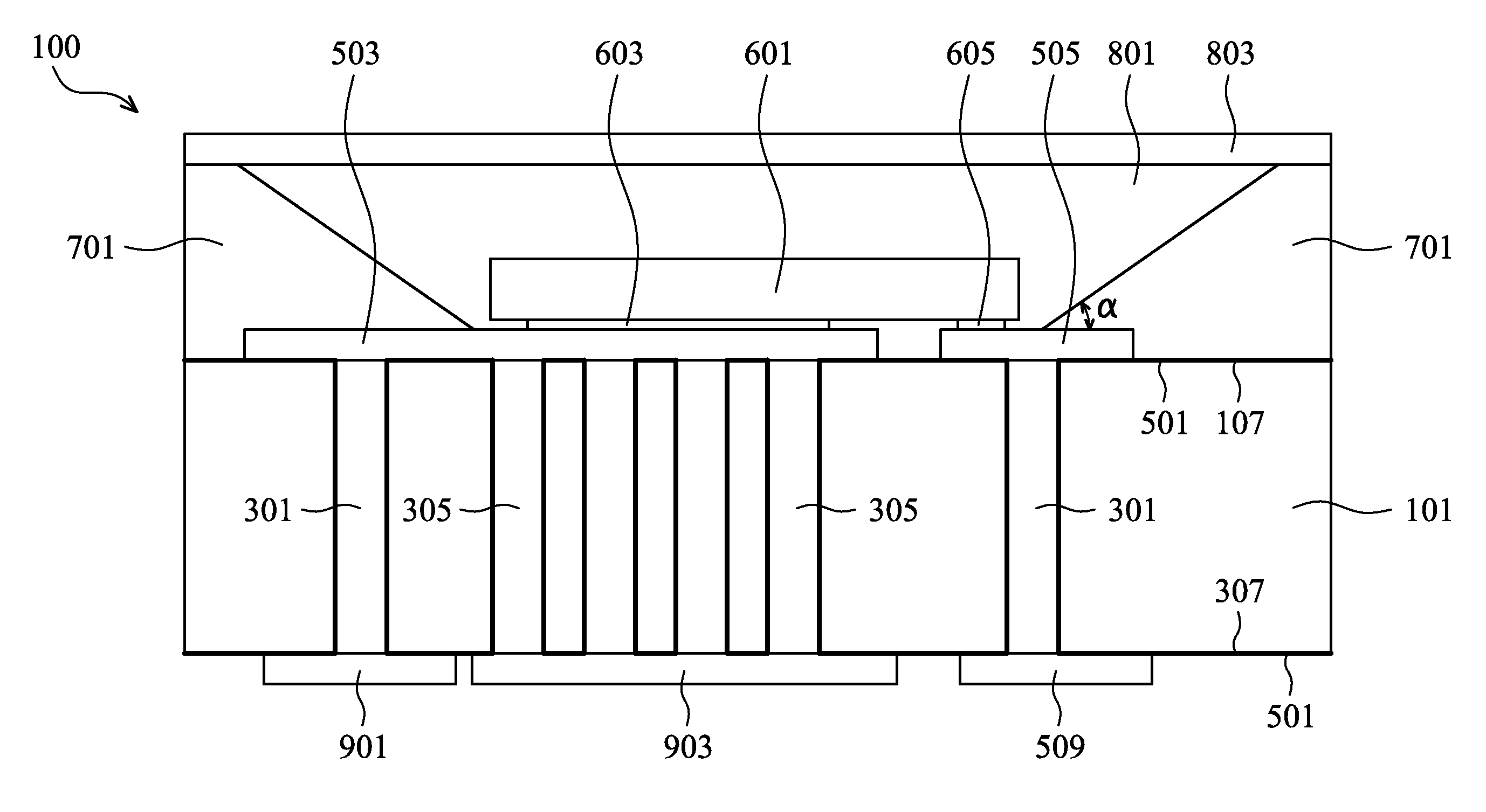
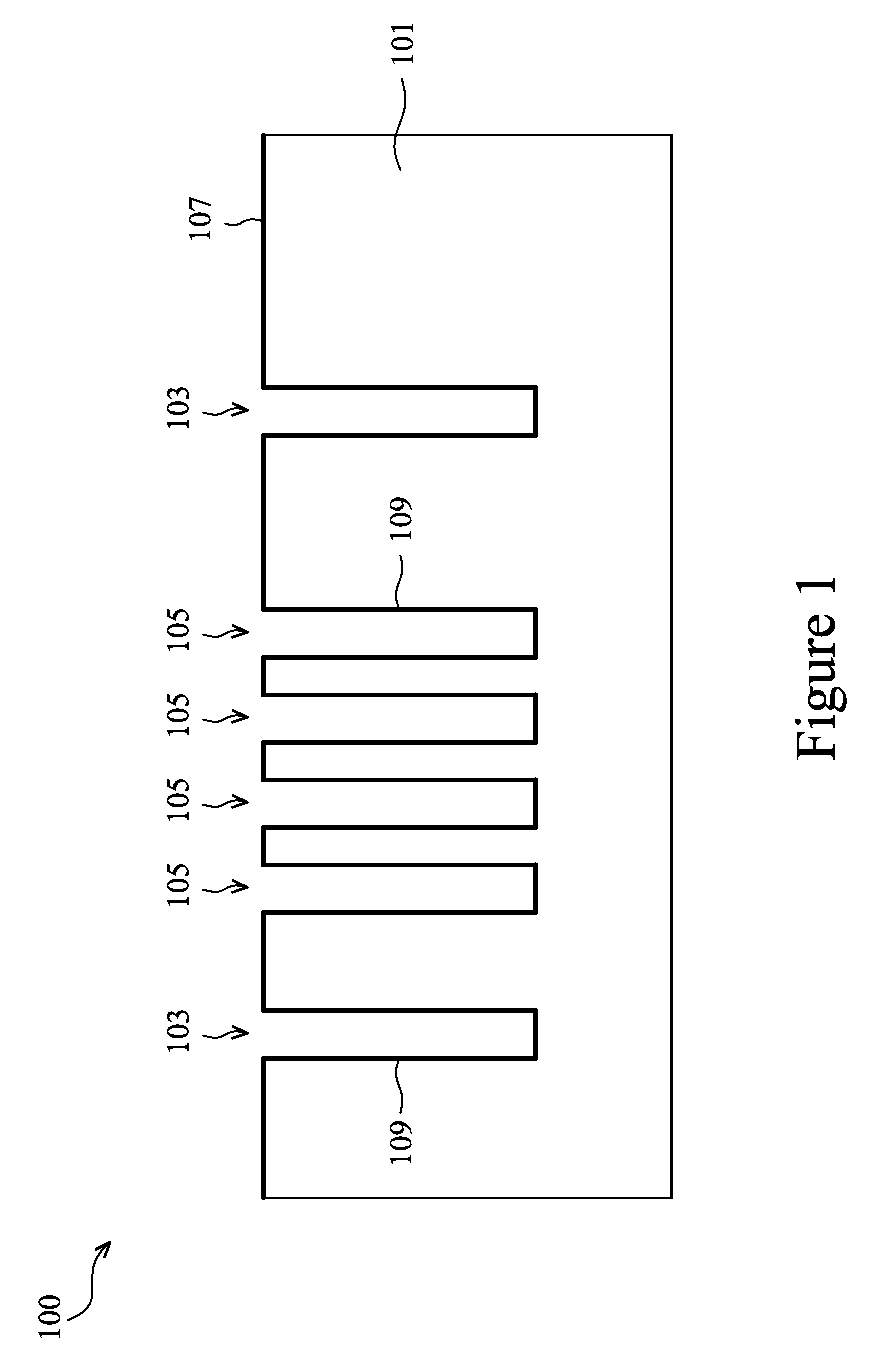
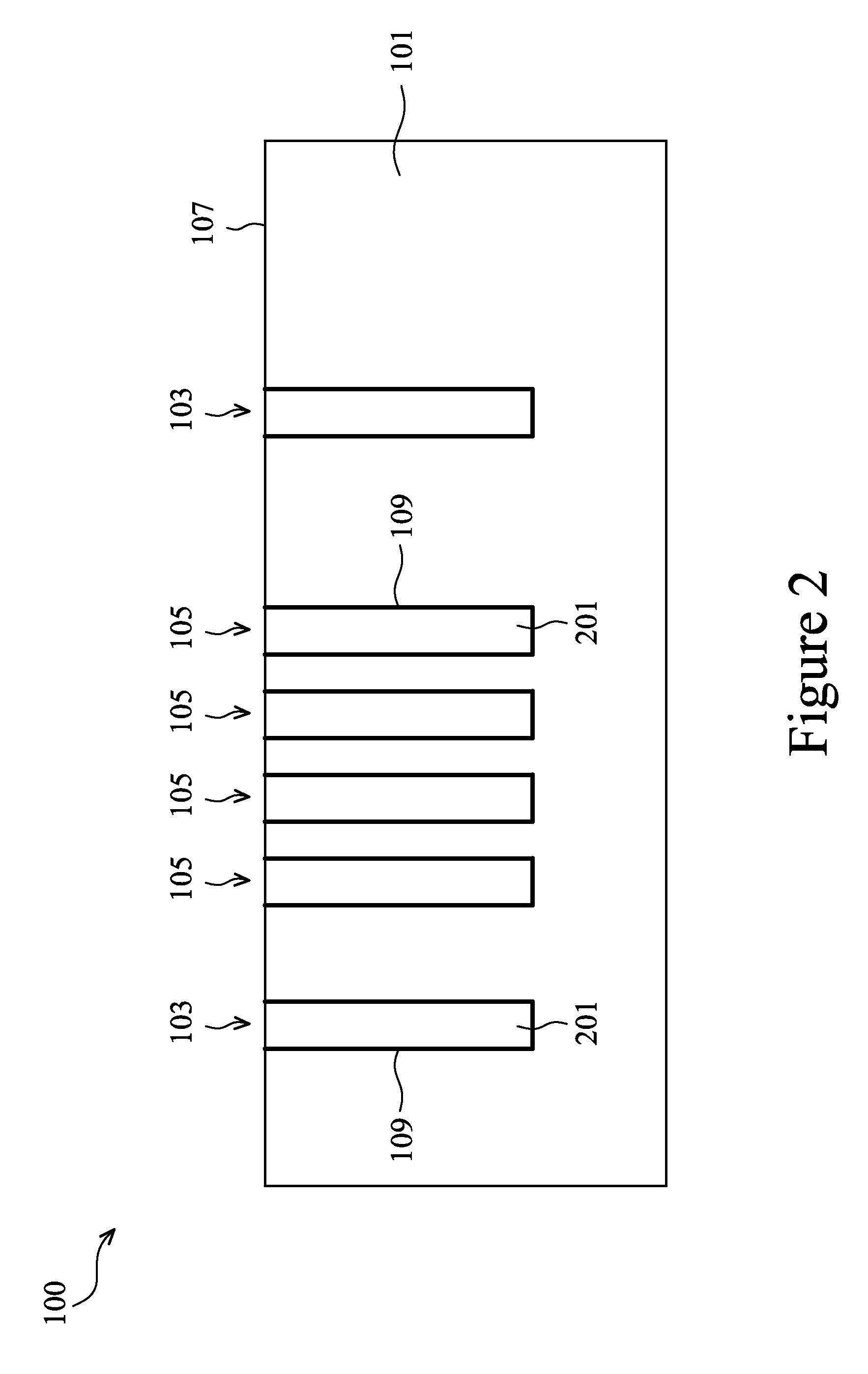
[0019]With reference now to FIG. 1, there is shown a cross-sectional view of a package 100 with a substrate 101 with contact openings 103 and thermal openings 105 formed therein. The substrate 101 may comprise bulk silicon, doped or undoped, or an active layer of a silicon-on-insulator (SOI) substrate. Generally, an SOI substrate comprises a...


PUM


Abstract

System and method for packaging an LED is presented. A preferred embodiment includes a plurality of thermal vias located through the packaging substrate to effectively transfer heat away from the LED, and are preferably formed along with conductive vias that extend through the packaging substrate. The thermal vias are preferably in the shape of circles or rectangular, and may either be solid or else may encircle and enclose a portion of the packaging substrate.

Description

[0001]This application claims the benefit of U.S. Provisional Application No. 61 / 050,529, filed on May 5, 2008, entitled “LED Package Structure and Fabrication Method,” which application is hereby incorporated herein by reference.TECHNICAL FIELD[0002]The present invention relates generally to a system and method for light-emitting diodes (LEDs) and, more particularly, to a system and method for packaging LEDs.BACKGROUND[0003]Generally, the demand for LEDs, and especially high-brightness, high-power LEDs, has increased over the past years. However, high-brightness, high-power LEDs, while generating large amounts of light, also generate large amounts of heat which can cause thermal degradation of the characteristics of the LEDs and reduce the overall lifespan of the LEDs. Accordingly, this heat must be transferred away from the LED as quickly and efficiently as possible.[0004]Recent techniques in the packaging of LEDs have led to the use of packages that contain a silicon substrate. T...

Claims


Application Information

Patent Timeline
Patent Type & Authority Applications(United States)
IPC IPC(8): H01L33/00H01L33/48H01L33/64
CPCH01L33/486H01L33/62H01L2224/16H01L33/647H01L33/642
Inventor CHIOU, WEN-CHIHYU, CHEN-HUACHEN, DING-YUAN
Owner CHIP STAR
Why Eureka
Try Eureka