Eureka AIR delivers breakthrough ideas for toughest innovation challenges, trusted by R&D personnel around the world.

Solid state imaging apparatus, solid state imaging device driving method and camera

Inactive Publication Date: 2009-11-12
SONY CORP
View PDF1 Cites 0 Cited by
  • Summary
  • Abstract
  • Description
  • Claims
  • Application Information

AI Technical Summary

Benefits of technology

[0027]However, in the above mentioned examples of the dark signal level reducing techniques, the amount of charge that can be handled by the vertical transfer unit may be reduced or vertical transfer efficiency of the vertical transfer unit may be reduced.
[0028]That is, as shown by a relation between a middle bias voltage (VM) of a vertical transfer clock signal Vφ to be applied to a vertical transfer unit and the amount of charge that can be handled by the vertical transfer unit in FIG. 6B, the amount of charge that can be handled by the vertical transfer unit may be reduced by negatively biasing the middle bias voltage (VM) of the vertical transfer clock signal Vφ. In addition, as shown by a relation between a middle bias voltage (VM) of a vertical transfer clock signal Vφ to be applied to a vertical transfer unit and vertical transfer efficiency of the vertical transfer unit in FIG. 6C, the vertical transfer efficiency of the vertical transfer unit may be reduced by negatively biasing the middle bias voltage (VM) of the vertical transfer clock signal Vφ.

Problems solved by technology

However, in the above mentioned examples of the dark signal level reducing techniques, the amount of charge that can be handled by the vertical transfer unit may be reduced or vertical transfer efficiency of the vertical transfer unit may be reduced.
Therefore, in one example of the above mentioned dark signal level reducing technique, although dark signal level reduction is attained, the quantity of saturating signals is reduced and defective vertical transfer is liable to occur as the amount of charge that can be handled by the vertical transfer unit is reduced and as a result of which the increase in SN ratio may not be expected.
In addition, the middle bias voltage (VM) of the vertical transfer clock signal Vφ to be applied to the vertical transfer unit is negatively biased for the entire time period ranging from the light-exposing time period to the signal outputting time period, so that defective vertical transfer may occur in a mode in which an image is displayed on a liquid crystal monitor (hereinafter, referred to as a liquid crystal monitor image displaying mode) and a moving image capturing mode necessitating high-speed transfer of signals charges using the vertical transfer unit.

Method used


Image

  • Solid state imaging apparatus, solid state imaging device driving method and camera
  • Solid state imaging apparatus, solid state imaging device driving method and camera
  • Solid state imaging apparatus, solid state imaging device driving method and camera

Examples


Embodiment Construction

[0052]Next, preferred embodiments of the present invention will be described with reference to the accompanying drawings.

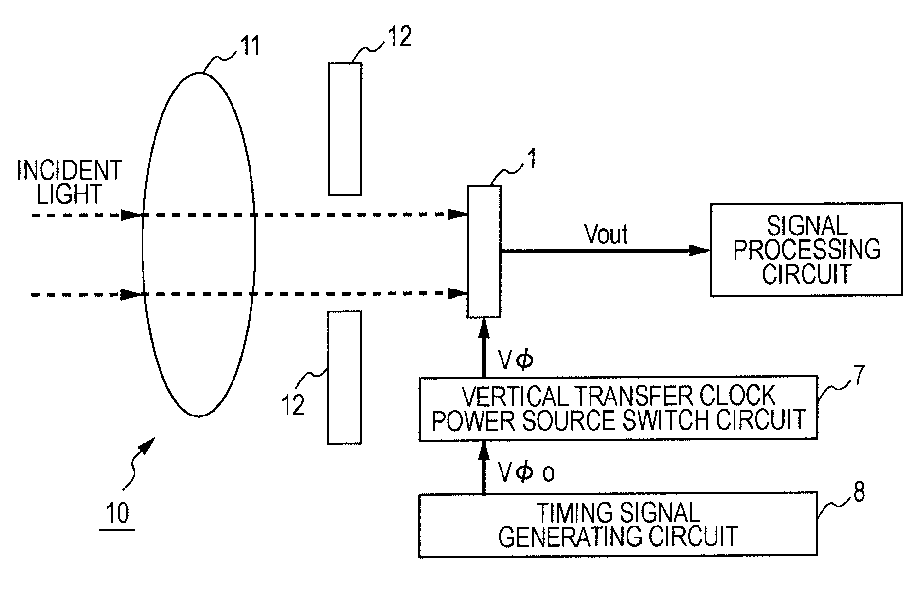
[0053]FIG. 1 is a schematic diagram illustrating a CCD type camera showing an example of a camera to which an embodiment of the present invention is applied. A CCD type camera 10 shown in the drawing includes a lens 11 configured to focus incident light, a mechanical shutter 12 configured to pass the light focused through the lens 11 only for a predetermined time period and a CCD type image sensor 1 configured to capture an image of a subject which is projected through the lens 11 and the mechanical shutter 12.

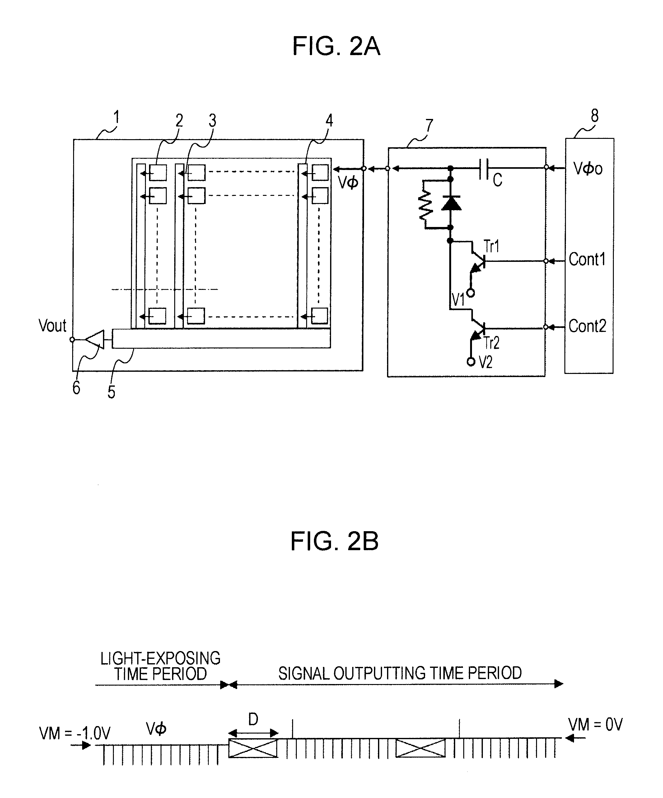
[0054]FIG. 2A is a schematic diagram illustrating a CCD type image sensor showing an example of a solid state imaging apparatus to which an embodiment of the present invention is applied. In a CCD type image sensor 1 shown in the drawing, a plurality of light sensing units 2 arrayed in a matrix, a read-out gate 3 disposed adjacent to each light sensing unit ...


PUM


Abstract

A solid state imaging apparatus includes a solid state imaging device and a control circuit for performing control such that a first clock signal applied to transfer signal charges for a time period from after a preceding signal charge has been read out from a light sensing unit to when the preceding signal charge is transferred to a horizontal transfer unit and a second clock signal applied for a time period from after the preceding signal charge has been transferred to the horizontal transfer unit to when a succeeding signal charge is read out from the light sensing unit have almost the same amplitude and a high level potential of the first clock signal is set higher than that of the second clock signal.

Description

BACKGROUND OF THE INVENTION[0001]1. Field of the Invention[0002]The present invention relates to a solid state imaging apparatus, a solid state imaging device driving method and a camera and more particularly to a solid state imaging apparatus, a solid state imaging device driving method and a camera configured to realize dark signal level reduction.[0003]2. Description of the Related Art[0004]In a camera such as a digital still camera or a security camera, a CCD (Charge Coupled Device) type image sensor of an inter-line transfer system has been widely used.[0005]FIG. 3 is a schematic diagram illustrating a CCD type image sensor of the inter-line transfer system. In the example shown in FIG. 3, a CCD type image sensor 101 includes a plurality of light sensing units 102 arrayed in a matrix, a read-out gate 103 disposed adjacent to each light sensing unit and configured to read out a signal charge input using the light sensing unit, a vertical transfer unit 104 disposed adjacent to th...

Claims


Application Information

Patent Timeline
IPC IPC(8): H04N5/335H01L27/148H04N5/353H04N5/361H04N5/372H04N5/376
CPCH04N5/361H04N5/3728H04N5/372H04N25/63H04N25/73H04N25/71
Inventor TANAKA, HIROAKI
Owner SONY CORP
Why Eureka
Eureka Blog
Learn More