
Circuit substrate and light emitting diode package

Inactive Publication Date: 2009-11-19
EVERLIGHT ELECTRONICS (CHINA) CO LTD
View PDF14 Cites 21 Cited by
  • Summary
  • Abstract
  • Description
  • Claims
  • Application Information

AI Technical Summary

Benefits of technology

[0012]The present invention is directed to a light emitting diode (LED) package having lower manufacture cost.
[0051]As described above, in the present invention, the lead units are arranged in a high density and each of the lead units can be divided into at least three conductive structures. Thus, more lead units can be fabricated on a unit area of substrate and each lead unit can be divided into more conductive structures. In other words, more conductive structures can be fabricated on a unit area of substrate. Thereby, the manufacture cost of conductive structures is reduced in the present invention.

Problems solved by technology

Accordingly, the manufacture cost of the conductive structures is high.

Method used


Image

  • Circuit substrate and light emitting diode package
  • Circuit substrate and light emitting diode package
  • Circuit substrate and light emitting diode package

Examples


Embodiment Construction

[0059]Reference will now be made in detail to the present preferred embodiments of the invention, examples of which are illustrated in the accompanying drawings. Wherever possible, the same reference numbers are used in the drawings and the description to refer to the same or like parts.

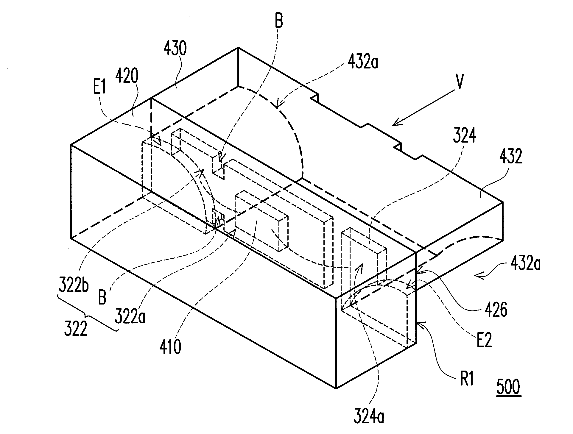
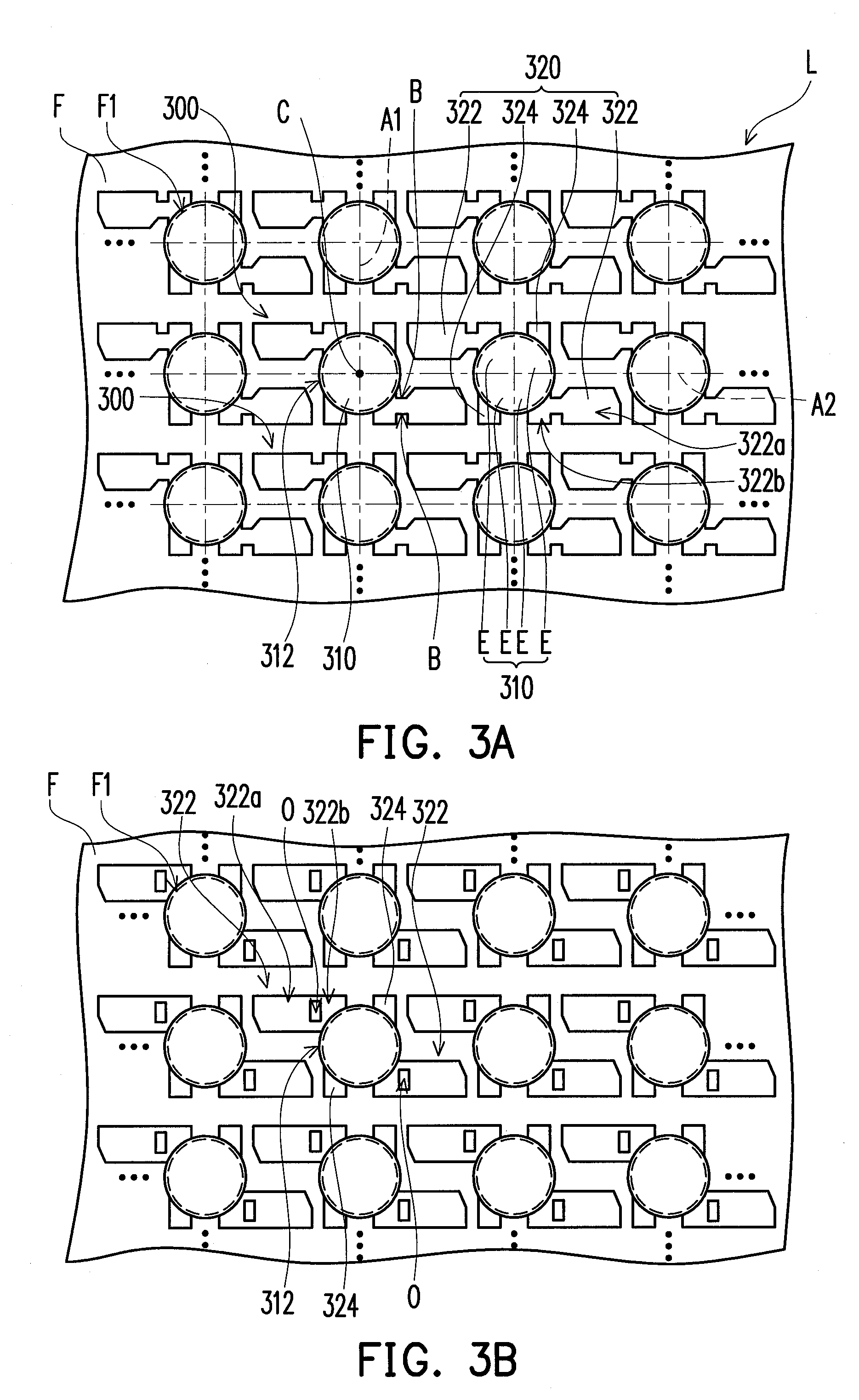
[0060]FIG. 3A and FIG. 3B are diagrams of a circuit substrate according to an embodiment of the present invention, and FIGS. 4˜11 illustrate different variations of the circuit substrate in FIG. 3A.

[0061]Referring to FIG. 3A, in the present embodiment, the circuit substrate L includes a base layer F and a plurality of lead units 300 arranged as an array, wherein the lead units 300 are all disposed on the base layer F and arranged into multiple rows and multiple columns on the base layer F. The base layer F has a plurality of through holes F1. Each of the lead units 300 includes a common terminal 310 and at least three leads 320. In the present embodiment, each of the lead units 300 has four leads 320...


PUM


Abstract

A circuit substrate including a base layer and a plurality of lead units arranged as an array is provided, wherein the base layer has a plurality of through grooves, and the lead units are disposed on the base layer. Each of the lead units includes a common terminal and at least three leads. The common terminal is capable of being divided into a plurality of electrodes connected with each other. The leads are extended outwards from the edge of the common terminal, and each of the leads is extended outwards from the edge of one of the electrodes. The through grooves expose the common terminals of the lead units.

Description

CROSS-REFERENCE TO RELATED APPLICATION[0001]This application claims the priority benefit of Taiwan application serial no. 97117902, filed May 15, 2008. The entirety of the above-mentioned patent application is hereby incorporated by reference herein and made a part of specification.BACKGROUND OF THE INVENTION[0002]1. Field of the Invention[0003]The present invention generally relates to a circuit substrate and a light emitting diode (LED) package, and more particularly, to a circuit substrate and a LED package having low manufacture cost.[0004]2. Description of Related Art[0005]Compared to the conventional light bulbs, light emitting diode (LED) has smaller volume, longer lifespan, lower energy consumption, and less contamination. Thus, LED has gradually replaced fluorescent lamp and incandescent lamp in some fields along with the advancement in the illumination efficiency thereof. For example, LED has been broadly applied to the light source of scanner which requires quick response...

Claims


Application Information

Patent Timeline
IPC IPC(8): H01L33/00H05K1/11
CPCH01L33/62H01L2224/48091H01L33/483H01L2924/00014G02F1/133603G02B6/009H01L2924/12041H01L51/5237F21Y2101/02H05K2201/10106H05K2201/10977
Inventor TSOU, WEN-CHIEH
Owner EVERLIGHT ELECTRONICS (CHINA) CO LTD
Features
  • Generate Ideas
  • Intellectual Property
  • Life Sciences
  • Materials
  • Tech Scout
  • Unparalleled Data Quality
  • Higher Quality Content
  • 60% Fewer Hallucinations
Learn More