
Two-Dimensional Photonic Crystal Surface Emitting Laser Light Source

a photonic crystal surface and laser light source technology, applied in lasers, optical beam sources, semiconductor lasers, etc., can solve the problems of reducing the lasing efficiency, generating heat, leaking light is absorbed by the active layer, etc., and achieve the effect of improving the light use efficiency

Active Publication Date: 2009-11-19
KYOTO UNIV +1
View PDF2 Cites 16 Cited by
  • Summary
  • Abstract
  • Description
  • Claims
  • Application Information

AI Technical Summary

Benefits of technology

[0026]The two-dimensional photonic crystal surface emitting laser light sources (which are hereinafter called the “surface emitting laser”) according to the first and second aspects of the invention each exhibit the following effect resulting from the structure of the reflector.
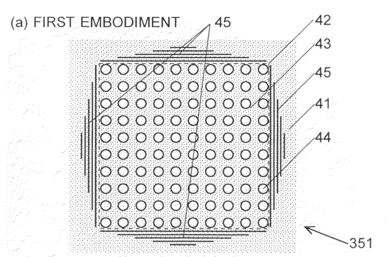
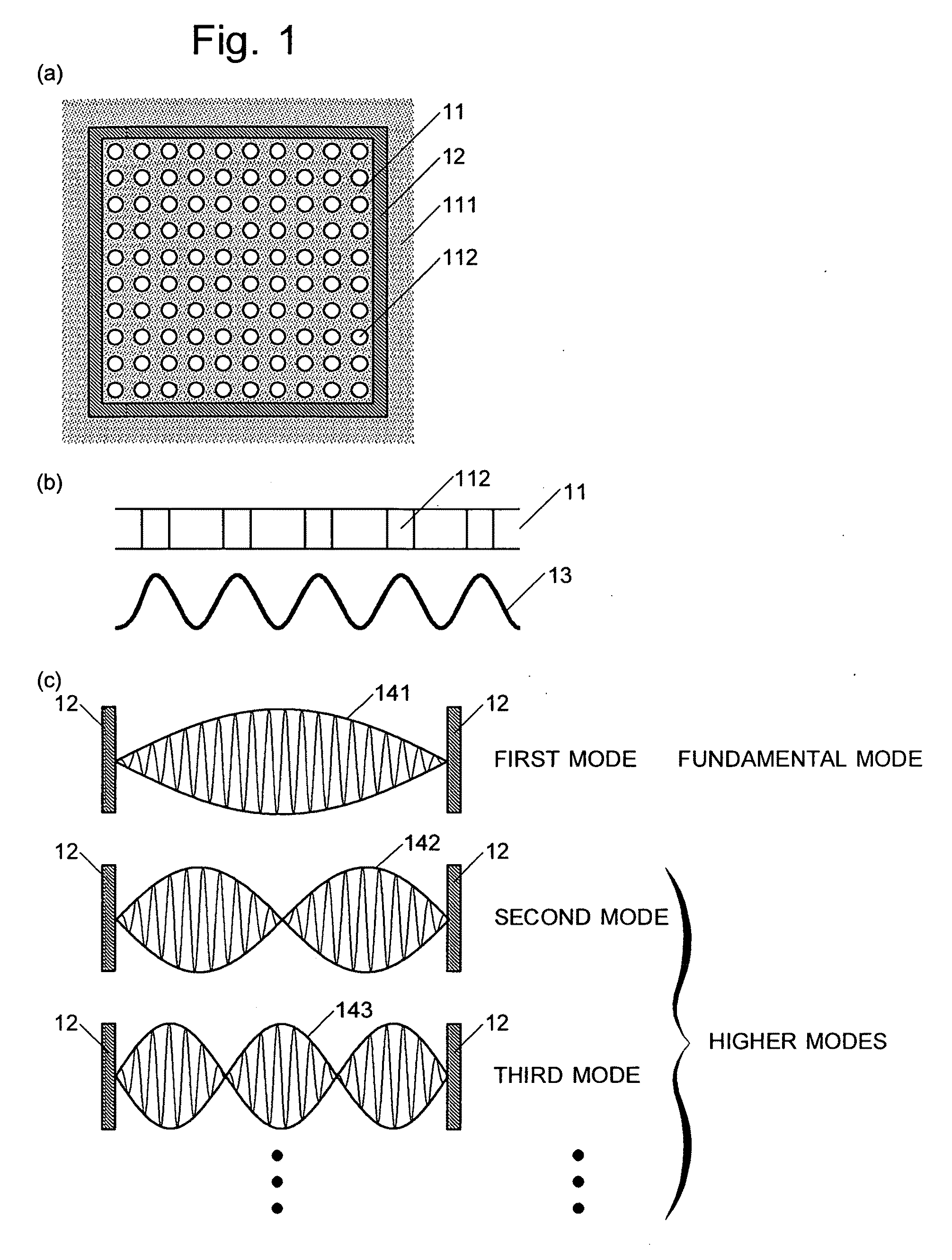
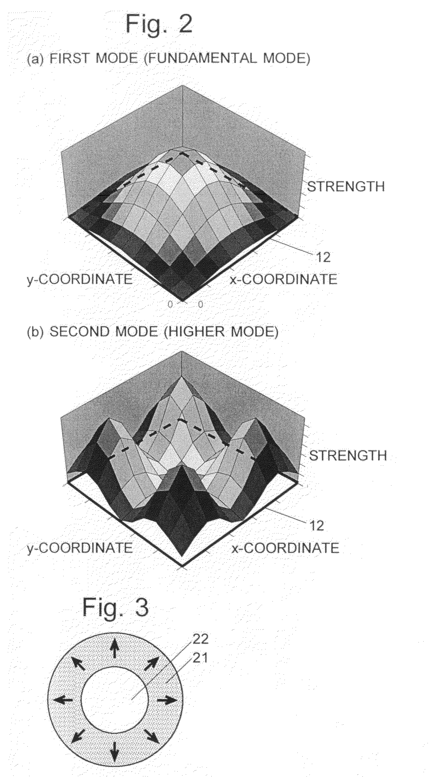
[0027]In the first aspect of the present invention, the presence of the reflector enables the surface emitting laser to improve a light use efficiency as in the case of the surface emitting laser disclosed in Patent Document 2. The reflector is designed so that its reflectance distribution has a maximum value at a position where the amplitude envelope of the fundamental mode has a maximum value. This design enables the laser oscillation in the fundamental mode to be selectively obtained, so that a single-wavelength laser light, which cannot be produced by the surface emitting laser in Patent Document 2, can be emitted.
[0028]Oscillation of higher order modes apts to be flanked by those of neighboring higher and lower modes. Therefore, the fundamental mode, i.e. the lowest order mode, is selected in the present invention.
[0029]The reflector may be provided only at one or more sections of a line surrounding the two-dimensional photonic crystal, the section including the position where the amplitu

Problems solved by technology

This leads to an energy loss and accordingly lowers the lasing efficiency.
Furthermore, the leaked light is absorbed by the active layer and generates

Method used


Image

  • Two-Dimensional Photonic Crystal Surface Emitting Laser Light Source
  • Two-Dimensional Photonic Crystal Surface Emitting Laser Light Source
  • Two-Dimensional Photonic Crystal Surface Emitting Laser Light Source

Examples


embodiments

(1) Embodiment of Surface Emitting Laser According to First Aspect of Invention

[0084]An embodiment of the surface emitting laser according to the first aspect of the present invention is hereinafter described with reference to FIGS. 4 to 11.

[0085]FIG. 4 is a perspective view of the laser light source in the present embodiment. This laser light source includes a substrate 31 made of an n-type semiconductor of gallium arsenide (GaAs), on which an active layer 33 made of indium gallium arsenide (InGaAs) / gallium arsenide (GaAs) and having multiple-quantum wells (MQW) is located, with a cladding layer 321 made of an n-type semiconductor of aluminum gallium arsenide (AlGaAs) in between. Provided on this active layer 33 is a two-dimensional photonic crystal layer 35, with a carrier-blocking layer 34 made of AlGaAs in between. The structure of the two-dimensional photonic crystal layer 35 will be later described. On this two-dimensional photonic crystal layer 35, a cladding layer 322 of p-A...


PUM


Abstract

An objective of the present invention is to provide a surface emitting laser capable of selectively generating a laser oscillation in the fundamental mode and thereby emitting a single-wavelength laser light. In a surface emitting laser including an active layer and a two-dimensional photonic crystal provided on one side of the active layer, a reflector 45 or 46 is provided at least at a portion of the circumference of the two-dimensional photonic crystal. The reflector has a reflectance distribution in which the reflectance has a maximum value at a position where the amplitude envelope of the fundamental mode of an internal resonance light created within the two-dimensional photonic crystal. This design strengthens the fundamental mode while suppressing the second mode, thus enabling the laser oscillation in the fundamental mode to be selectively obtained, so that a single-wavelength laser light can be emitted.

Description

TECHNICAL FIELD[0001]The present invention relates to a two-dimensional photonic crystal surface emitting laser light source which emits laser light in a direction perpendicular to the surface of a flat light source.BACKGROUND ART[0002]In recent years, new types of laser light sources using a photonic crystal have been developed. A photonic crystal consists of a dielectric body material in which an artificial periodic structure is created. Usually, the periodic structure is created by providing the body material with a periodic arrangement of areas whose refractive index differs from that of the body material (this area is hereinafter called the “modified refractive index area”). The periodic structure causes a Bragg diffraction within the crystal and creates an energy band gap for the energy of light. There are two types of photonic crystal laser light sources: one utilizes a band-gap effect to make a point-like defect function as a resonator, and the other utilizes a standing wave...

Claims


Application Information

Patent Timeline
IPC IPC(8): H01S5/183H01S5/185
CPCB82Y20/00G11B7/127H01S5/0425H01S5/105H01S2301/18H01S5/18H01S5/2027H01S5/34313H01S2301/14H01S5/125H01S5/11H01S5/185
Inventor SAKAI, KYOSUKEMIYAI, EIJINODA, SUSUMUOHNISHI, DAIKUNISHI, WATARU
Owner KYOTO UNIV
Learn More