Optical device, projector, and method of producing optical device

a technology of optical devices and projectors, applied in the direction of lenses, diffusing elements, instruments, etc., can solve the problems of general inefficiency in using light, insufficient correction of intensity distribution of beam flux,

Active Publication Date: 2015-10-15
ASAHI GLASS CO LTD
View PDF46 Cites 34 Cited by
  • Summary
  • Abstract
  • Description
  • Claims
  • Application Information

AI Technical Summary

Benefits of technology

[0007]According to an aspect of the present invention, an optical device includes a base material including a surface on which multiple concaves are formed. The concaves include respective curved surfaces. The concaves are formed so that the bottoms of the concaves are at two or more different positions in a depth

Problems solved by technology

The diffuser plate, however, diffuses light using random irregularities on its surface, and therefore, is generally inefficient in using light.
In the case of using a highly coherent light source such as a laser, the intensi

Method used


Image

  • Optical device, projector, and method of producing optical device
  • Optical device, projector, and method of producing optical device
  • Optical device, projector, and method of producing optical device

Examples


first embodiment

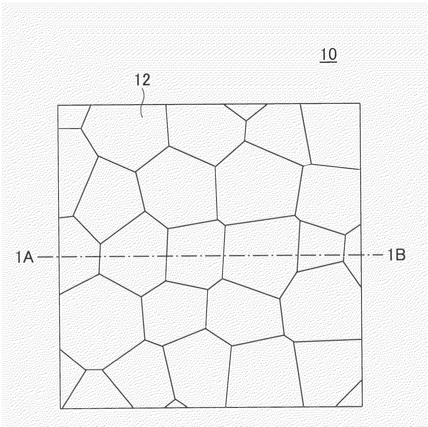
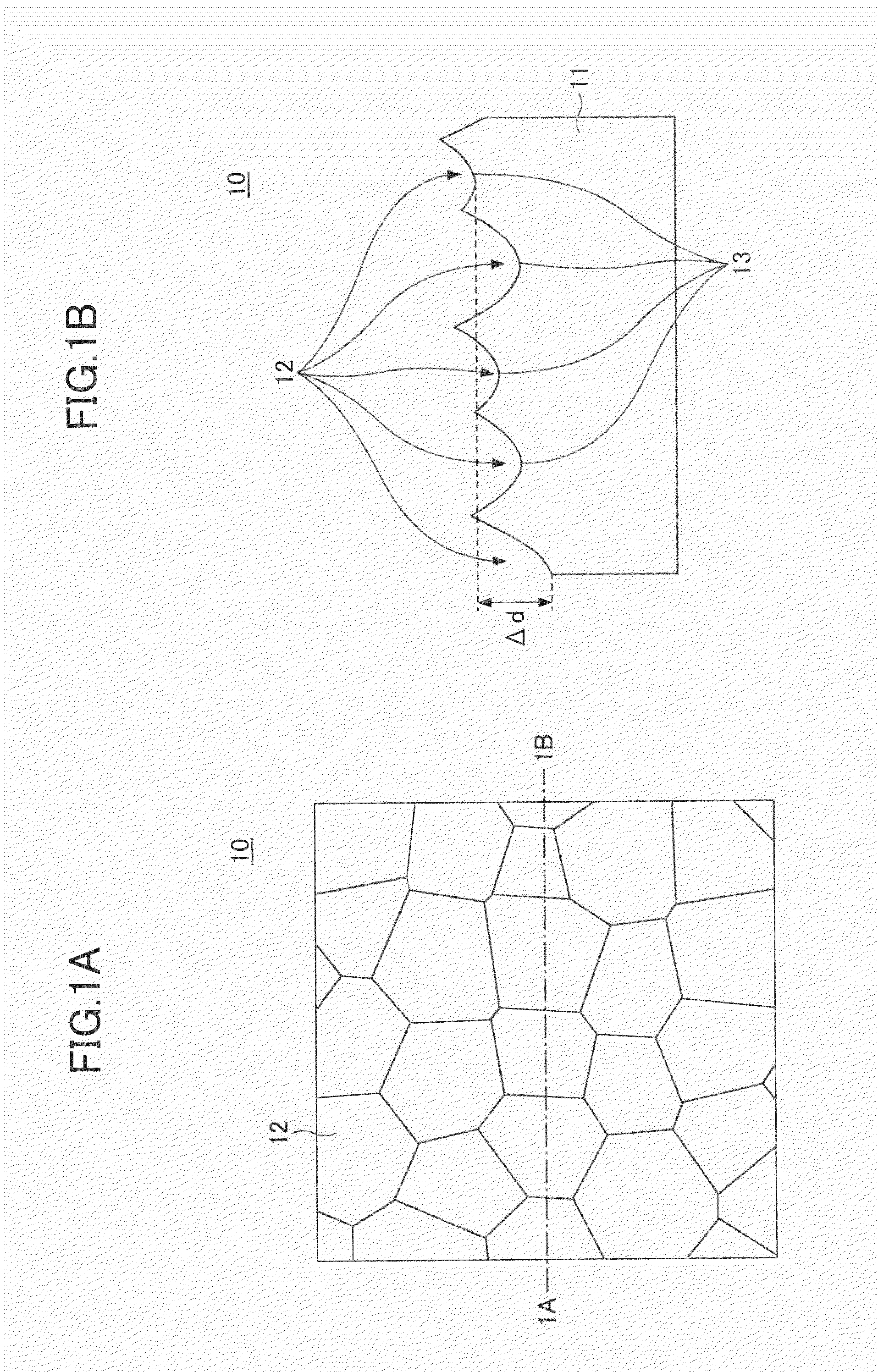
[0076]The above-described microstructures according to U.S. Pat. No. 7,033,736, which are widely distributed in the depth direction, may generate unnecessary scattered light in the case of light that obliquely enters, such as diverging light.

[0077]Furthermore, resistance to light may be required when laser light is caused to enter. Therefore, optical devices are preferably formed using a light resistant material such as glass as a base material. One method of making a surface of glass or the like uneven is wet etching. In general, however, the shapes that may be formed by wet etching are limited. In the case of forming an uneven surface with deep concaves that differ in depth as illustrated in U.S. Pat. No. 7,033,736, it is difficult to form a desired shape with wet etching.

[0078]Other methods of making a surface of glass or the like uneven include dry etching and press forming. In the case of forming an uneven surface with deep concaves, however, the dry etching has the problem of ...

example 1

[0161]First, a description is given, with reference to FIGS. 13A through 13D, of an optical device according to Example 1.

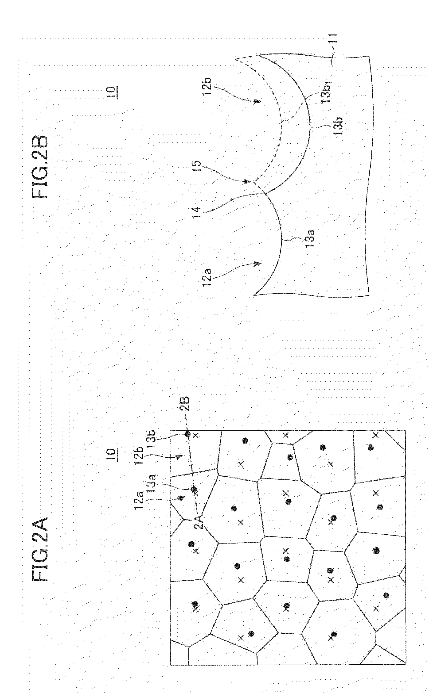
[0162]The base material 11 formed of glass of a refractive index of 1.53 is cleaned, and a molybdenum film of 50 nm in thickness is deposited on the base material 11 as the mask 21. After deposition of the molybdenum film, a resist is applied, and openings of 1 μm in diameter are formed in the mask 21 by photolithography and etching so as to be arranged as illustrated in FIG. 13A. FIG. 13A illustrates the positions of openings within an area of approximately 1 mm square, where the openings are arranged in a plane at a pitch of 50 μm so that the nearest openings are connected to form equilateral triangles. After formation of the openings, wet etching of 480 μm is performed. Accordingly, the curved surface 24 in the concave 12 has a radius of curvature of 480 μm. FIG. 13B illustrates a planar shape of the optical device after processing. In FIG. 13B, the depth is i...

example 2

[0164]Next, a description is given, with reference to FIGS. 14A through 14D, of an optical device according to Example 2, focusing on differences from that of Example 1.

[0165]Openings of 1 μm in diameter are formed in the mask 21 so as to be arranged as illustrated in FIG. 14A. FIG. 14A illustrates the positions of openings within an area of approximately 1 mm square, where a positional irregularity of the value of 25% of the pitch is introduced into such an arrangement of openings in a plane at a pitch of 50 μm that the nearest openings are connected to form equilateral triangles. After formation of the openings, wet etching of 480 μm is performed. Accordingly, the curved surface 24 in the concave 12 has a radius of curvature of 480 μm. FIG. 14B illustrates a planar shape of the optical device after processing. In FIG. 14B, the depth is illustrated in grayscale, so that the color becomes darker as the depth increases.

[0166]FIG. 14C illustrates a result of calculation of an exiting ...


PUM


Abstract

An optical device includes a base material including a surface on which multiple concaves are formed. The concaves include respective curved surfaces. The concaves are formed so that the bottoms of the concaves are at two or more different positions in a depth direction. In the optical device, 2/7≦|(n1−n2)×Δd|/λ≦10 holds, where n1 is the refractive index of the base material, n2 is the refractive index of a medium around the concaves, λ is the wavelength of a beam flux that enters the base material, and Δd is a range of the positions of the bottoms in the depth direction.

Description

CROSS-REFERENCE TO RELATED APPLICATIONS[0001]The present application is a continuation application filed under 35 U.S.C. 111(a) claiming benefit under 35 U.S.C. 120 and 365(c) of PCT International Application No. PCT / JP2013 / 084693, filed on Dec. 25, 2013 and designating the U.S., which claims priority to Japanese Patent Applications No. 2012-287196, filed on Dec. 28, 2012, No. 2013-143561, filed on Jul. 9, 2013, No. 2013-167565, filed on Aug. 12, 2013, and No. 2013-189364, filed on Sep. 12, 2013. The entire contents of the foregoing applications are incorporated herein by reference.BACKGROUND OF THE INVENTION[0002]1. Field of the Invention[0003]The present invention relates to optical devices, projectors, and methods of producing optical devices.[0004]2. Description of the Related Art[0005]Some projectors that employ a laser as a light source use such a diffuser plate as disclosed in Japanese Laid-Open Patent Application No. 2007-233371 in order to correct the intensity distribution...

Claims


Application Information

Patent Timeline
IPC IPC(8): G02B3/00G03B21/20G03B21/00
CPCG02B3/0037G03B21/2033G03B21/005G02B5/0221G02B5/02G02B5/0215G02B5/0226G02B5/0231G02B5/0268G02B5/0278G03B21/204G03B21/208G03B33/06G03B33/12H04N9/3152
Inventor MIYASAKA, KOJIYAMASHITA, SHUICHI
Owner ASAHI GLASS CO LTD
Why Eureka
Try Eureka