Method for electronically pinning a back surface of a back-illuminated imager fabricated on a utsoi wafer

a back surface and imager technology, applied in the manufacture of semiconductor/solid-state devices, semiconductor devices, electrical equipment, etc., can solve the problems of reducing the overall efficiency and sensitivity of the device, adding to the complexity of the fabrication process, and methods that cannot be easily included in conventional semiconductor foundry processing

Active Publication Date: 2009-12-03
SRI INTERNATIONAL
View PDF19 Cites 9 Cited by
  • Summary
  • Abstract
  • Description
  • Claims
  • Application Information

AI Technical Summary

Problems solved by technology

It is also desirable to minimize the recombination of the generated carriers before they reach the front side, since such recombination reduces overall efficiency and sensitivity of the device.
This requires additional treatment at the backside of the device, which adds to complexity of the fabrication process.
These methods can not be easily included in conventional semiconductor foundry processing, and require more expensive custom processing.
They are therefore often not cost-effective and not suitable for commercial manufacturing.
However, the hig

Method used


Image

  • Method for electronically pinning a back surface of a back-illuminated imager fabricated on a utsoi wafer
  • Method for electronically pinning a back surface of a back-illuminated imager fabricated on a utsoi wafer
  • Method for electronically pinning a back surface of a back-illuminated imager fabricated on a utsoi wafer

Examples


Embodiment Construction

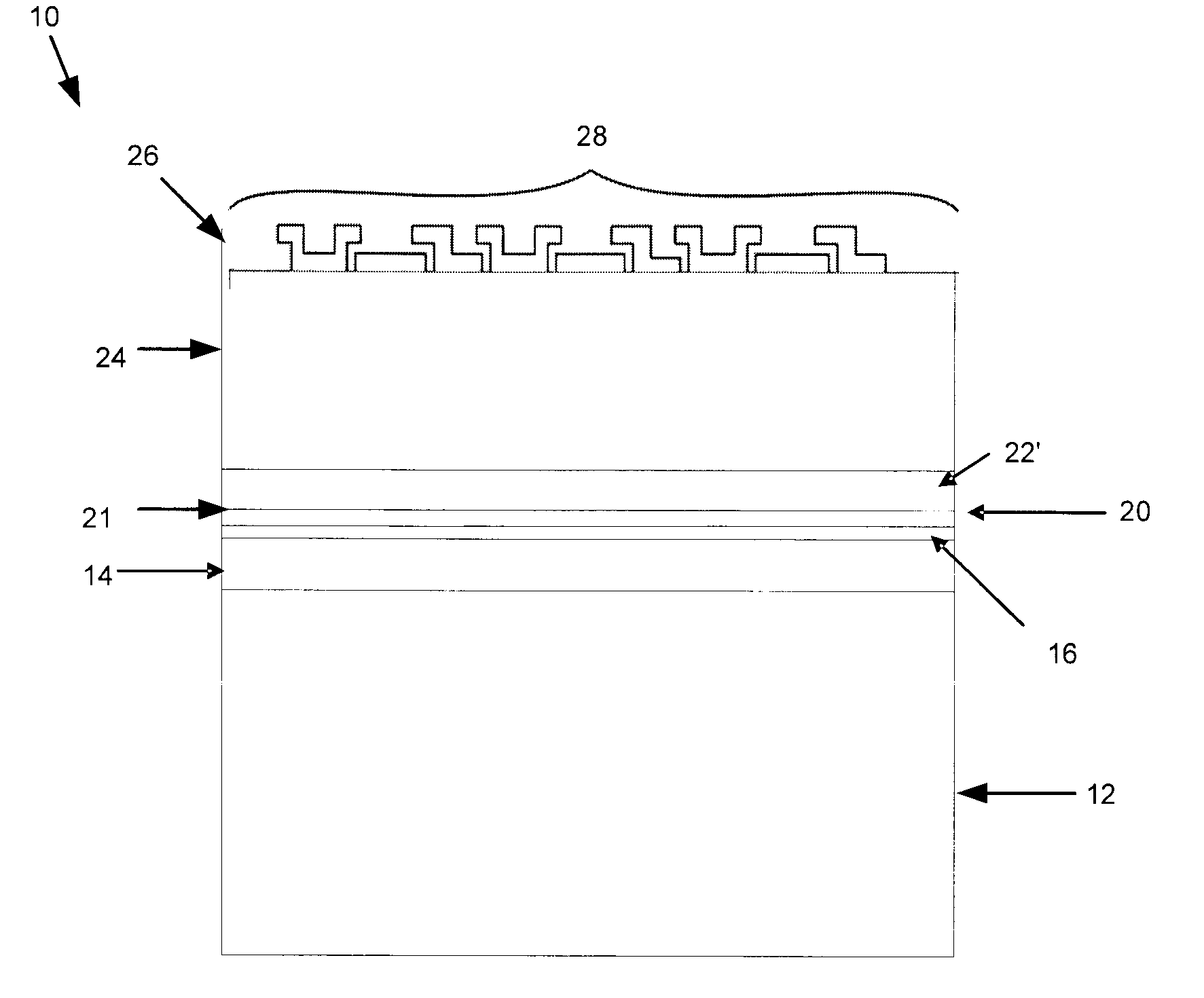
[0028]FIG. 3 shows an exemplary pinned back-illuminated UTSOI imager 10, constructed in accordance with an illustrative embodiment of the present invention. The UTSOI imager 10 initially includes a mechanical substrate 12, composed of any suitable material, such as, for example, silicon. A first insulator layer 14 (e.g., an oxide of silicon layer) overlies the mechanical substrate 12. A thin conductive layer 16, preferably made of metal, overlies the first insulator layer 14. According to an embodiment of the present invention, the conductive (metal) layer 16 has a thickness in the range of between 25-30 Angstroms. In this thickness range, the conductive layer 16 may be optically transparent. In other embodiments, the conductive layer 16 may be made of doped polysilicon.

[0029]A second insulator layer 20, preferably made of an oxide of silicon, overlies the conductive layer 16. A seed layer 22, preferably made of silicon, is formed overlying the second insulator layer 20 by a process...


PUM


Abstract

A method for fabricating a back-illuminated imager which has a pinned back surface is disclosed. A first insulator layer is formed overlying a mechanical substrate. A conductive layer is deposited overlying the first insulator layer. A second insulator layer is formed overlying the conductive layer to form a first structure, an interface being formed between the conductive layer and the second insulator layer, the conductive layer causing band bending proximal to the interface such that the interface is electrically pinned. Hydrogen is implanted in a separate device wafer to form a bubble layer. A final insulator layer is formed overlying the device wafer to form a second structure. The first structure and the second structure are bonded to form a combined wafer. A portion of the combined wafer is removed underlying the bubble layer to expose a seed layer comprising the semiconductor material substantially overlying the second insulator layer.

Description

CROSS-REFERENCE TO RELATED APPLICATIONS[0001]This application claims the benefit of U.S. provisional patent application No. 61 / 057,320 filed May 30, 2008, the disclosure of which is incorporated herein by reference in its entirety.FIELD OF THE INVENTION[0002]The field of invention is semiconductor device fabrication and device structure. More specifically, the field is fabrication and structure of back-illuminated semiconductor imaging devices that employ ultra-thin silicon on insulator (UTSOI) substrates, wherein the back surface of the imaging devices are electrically pinned.BACKGROUND OF THE INVENTION[0003]Thinned, back illuminated, semiconductor imaging devices are advantageous over front-illuminated imagers for high fill factor and better overall efficiency of charge carrier generation and collection. A desired property of such devices is that the charge carriers generated by light or other emanation incident on the back side should be driven to the front side quickly to avoid ...

Claims


Application Information

Patent Timeline
IPC IPC(8): H01L31/101H01L31/18H01L21/30
CPCH01L21/84H01L27/1464H01L27/14687
Inventor SWAIN, PRADYUMNA KUMARCHESKIS, DAVID JAYBHASKARAN, MAHALINGAM
Owner SRI INTERNATIONAL
Why Eureka
Try Eureka