Gallium nitride-based light emitting diode structure and preparation method therefor

A light-emitting diode, gallium nitride-based technology, applied in nanotechnology, semiconductor devices, electrical components, etc. for materials and surface science, can solve the problems of reducing light absorption effect, antistatic ability, voltage rise, etc. Resistance, uniformity increase, effect of voltage decrease

Active Publication Date: 2017-05-31
ANHUI SANAN OPTOELECTRONICS CO LTD
View PDF3 Cites 7 Cited by
  • Summary
  • Abstract
  • Description
  • Claims
  • Application Information

AI Technical Summary

Problems solved by technology

At present, in addition to continuously adjusting the technical process of the quantum well light-emitting layer, how to reduce the thickness of the P-type, thereby reducing the light absorption effect is also the main focus, but the decrease in thickness will lead to a decrease in antistatic ability and an increase in voltage. Therefore, how to control the P-type Materials and resistance are an important part of current research

Method used


Image

  • Gallium nitride-based light emitting diode structure and preparation method therefor
  • Gallium nitride-based light emitting diode structure and preparation method therefor
  • Gallium nitride-based light emitting diode structure and preparation method therefor

Examples


Embodiment 1

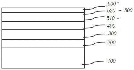
[0035] see figure 1 , the structure of a gallium nitride-based light-emitting diode implemented in the present invention and its preparation method will be described in detail below.

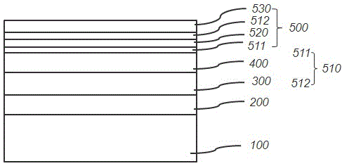
[0036] The LED structure of the present invention includes a substrate 100 , a bottom layer 200 , an N-type layer 300 , a light-emitting layer 400 and a P-type layer 500 . Wherein, the selection of the substrate 100 includes but is not limited to sapphire, aluminum nitride, gallium nitride, silicon, and silicon carbide, and its surface structure can be a planar structure or a patterned structure. In this embodiment, a patterned sapphire substrate is used. The P-type layer 500 is composed of an electron blocking layer 510, at least one energy band deforming layer 520, and a hole injection layer 530, wherein the electron blocking layer 510 can be selected as a single-layer pAlGaN structure containing Al elements or as a pAlGaN / pGaN supercrystal The lattice structure is either a pAlGaN / pInGaN / pGa...

Embodiment 2

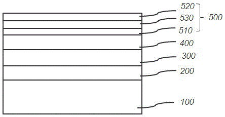
[0042] Continue to see attached Figure 1~5 , the difference between this embodiment and Embodiment 1 is that N-type doping is performed on the energy band deforming layer 520, and its impurity concentration is less than or equal to 8×10 16 cm -3 , the doping method is periodic, gradient doping, and band doping, which further enhances the bending degree of the energy band deforming layer 520 and enhances the concentration of two-dimensional hole gas.

Embodiment 3

[0044] Continue to see attached Figure 1~5 The difference between this embodiment and Embodiment 1 is that: add indium element to the energy band deforming layer 520 to form a non-doped u-InGaN material layer or an N-type doped n-InGaN material layer with lower potential energy, further Expand the potential energy difference between the energy band deforming layer 520 and the adjacent electron blocking layer 510 and / or hole injection layer 530, increase the bending degree of the energy band deforming layer 520, and strengthen the concentration of two-dimensional hole gas.


PUM


Abstract

Disclosed is a gallium nitride-based light emitting diode structure. The gallium nitride-based light emitting diode structure comprises a substrate, a bottom layer, an N type layer, a light emitting layer and a P type layer in sequence; the gallium nitride-based light emitting diode structure is characterized in that the P type layer consists of an electron barrier layer, at least one energy band deformation layer and a hole injection layer; the energy band deformation layer is inserted in the electron barrier layer or positioned between the electron barrier layer and the hole injection layer, or inserted in the hole injection layer or positioned on the hole injection layer; and the energy band deformation layer is a non-P type layer with carbon impurity content of not greater than 5*10<16>cm<-3>. By virtue of the low carbon impurity content, the energy band of the energy band deformation layer can be bent, and the two-dimensional hole gas concentration on a contact interface between the energy band deformation layer and the adjacent layer can be increased.

Description

technical field [0001] The invention relates to the technical field of semiconductors, in particular to a gallium nitride-based light-emitting diode structure and a preparation method thereof. Background technique [0002] The epitaxial wafer of a traditional GaN-based light-emitting diode includes a substrate, a buffer layer, an N-type layer, a multi-quantum well layer and a P-type layer grown sequentially on the substrate. As light-emitting diodes are more and more widely used, the brightness requirements of light-emitting diodes also increase accordingly. At present, in addition to continuously adjusting the technical process of the quantum well light-emitting layer, how to reduce the thickness of the P-type, thereby reducing the light absorption effect is also the main focus, but the decrease in thickness will lead to a decrease in antistatic ability and an increase in voltage. Therefore, how to control the P-type Materials and resistance are an important content of cur...

Claims


Application Information

Patent Timeline
Patent Type & Authority Applications(China)
IPC IPC(8): H01L33/02H01L33/14H01L33/16H01L33/00B82Y30/00
CPCB82Y30/00H01L33/0075H01L33/025H01L33/14H01L33/16
Inventor 李政鸿翁聪程志青林兓兓张家宏
Owner ANHUI SANAN OPTOELECTRONICS CO LTD
Why Eureka
Try Eureka