A gallium nitride-based light-emitting diode structure and its preparation method
A light-emitting diode, gallium nitride-based technology, applied in nanotechnology for materials and surface science, semiconductor devices, electrical components, etc., can solve the problems of reducing light absorption effect, decreasing antistatic ability, and increasing voltage, so as to reduce Effects of resistance, uniformity increase, and voltage reduction
- Summary
- Abstract
- Description
- Claims
- Application Information
AI Technical Summary
Problems solved by technology
Method used
Image
Examples
Embodiment 1
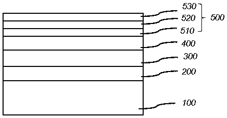
[0035] see figure 1 , the structure of a gallium nitride-based light-emitting diode implemented in the present invention and its preparation method will be described in detail below.
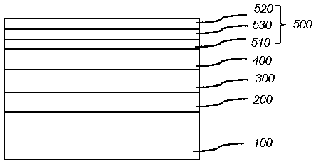
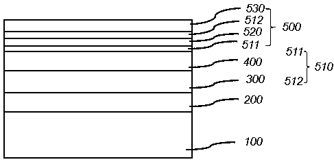
[0036] The LED structure of the present invention includes a substrate 100 , a bottom layer 200 , an N-type layer 300 , a light-emitting layer 400 and a P-type layer 500 . Wherein, the selection of the substrate 100 includes but is not limited to sapphire, aluminum nitride, gallium nitride, silicon, and silicon carbide, and its surface structure can be a planar structure or a patterned structure. In this embodiment, a patterned sapphire substrate is used. The P-type layer 500 is composed of an electron blocking layer 510, at least one energy band deforming layer 520, and a hole injection layer 530, wherein the electron blocking layer 510 can be selected as a single-layer pAlGaN structure containing Al elements or as a pAlGaN / pGaN supercrystal The lattice structure is either a pAlGaN / pInGaN / pGa...
Embodiment 2
[0042] Continue to see attached Figure 1-5 , the difference between this embodiment and Embodiment 1 is that N-type doping is performed on the energy band deforming layer 520, and its impurity concentration is less than or equal to 8×10 16 cm -3 , the doping method is periodic, gradient doping, and band doping, which further enhances the bending degree of the energy band deforming layer 520 and enhances the concentration of two-dimensional hole gas.
Embodiment 3
[0044] Continue to see attached Figure 1-5 The difference between this embodiment and Embodiment 1 is that: add indium element to the energy band deforming layer 520 to form a non-doped u-InGaN material layer or an N-type doped n-InGaN material layer with lower potential energy, further Expand the potential energy difference between the energy band deforming layer 520 and the adjacent electron blocking layer 510 and / or hole injection layer 530, increase the bending degree of the energy band deforming layer 520, and strengthen the concentration of two-dimensional hole gas.
PUM
 Abstract
Description
Claims
Application Information


