
Lead frame and semiconductor device utilizing the same

Inactive Publication Date: 2009-12-03
RENESAS ELECTRONICS CORP
View PDF17 Cites 0 Cited by
  • Summary
  • Abstract
  • Description
  • Claims
  • Application Information

AI Technical Summary

Benefits of technology

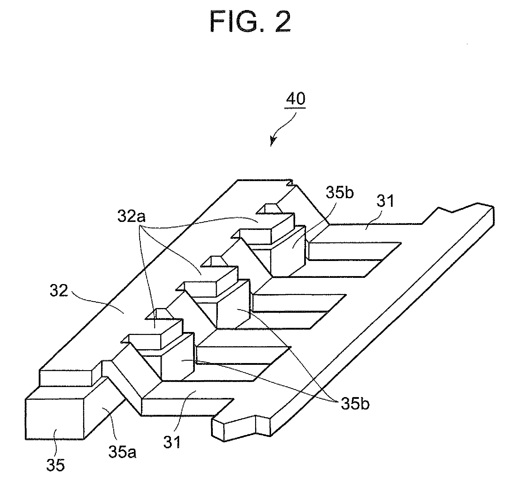
[0014]According to an embodiment of the present invention, the tip of the inner lead can be prevented from floating upward, because the mutual action of the extended section and extended section support piece act to receive and resist the tensile stress during clamping, since an extended, section is integrally extended from the inner lead toward the outer lead side and the bottom surface of this extended section is supported by the acceptor clamp jig even if the tensile stress pulls on the step during clamping of the outer lead. A drop in bonding strength can in this way be reduced during ultrasonic bonding of wires and bumps, since the ultrasonic waves are efficiently applied with no ultrasonic wave loss occurring in the joint or bond between the inner lead and wire or bump, etc.

Problems solved by technology

However, the following problems occur when the lead frame 30 is clamped.
Consequently, a loss of ultrasonic waves occurs in the joint between the inner lead 32 and the wire or bump during ultrasonic bonding such as of wires or bumps, so that the efficiency at which the ultrasonic waves are applied becomes worse and the joint strength deteriorates.
Though there are no particular restrictions on the shape, dimensions, or quantity of the extended sections, an extended section that is too short may fail to prevent upward floating of the inner lead tip that occurs due to tensile stress applied on the step difference section during clamping.

Method used


Image

  • Lead frame and semiconductor device utilizing the same
  • Lead frame and semiconductor device utilizing the same
  • Lead frame and semiconductor device utilizing the same

Examples


Embodiment Construction

[0034]The present invention will now be described herein with reference to the illustrative embodiments. Those skilled in the art will recognize that many alternative embodiments can be rendered by using the teachings of the present invention, and that the invention is not limited to the embodiments illustrated for descriptive purposes.

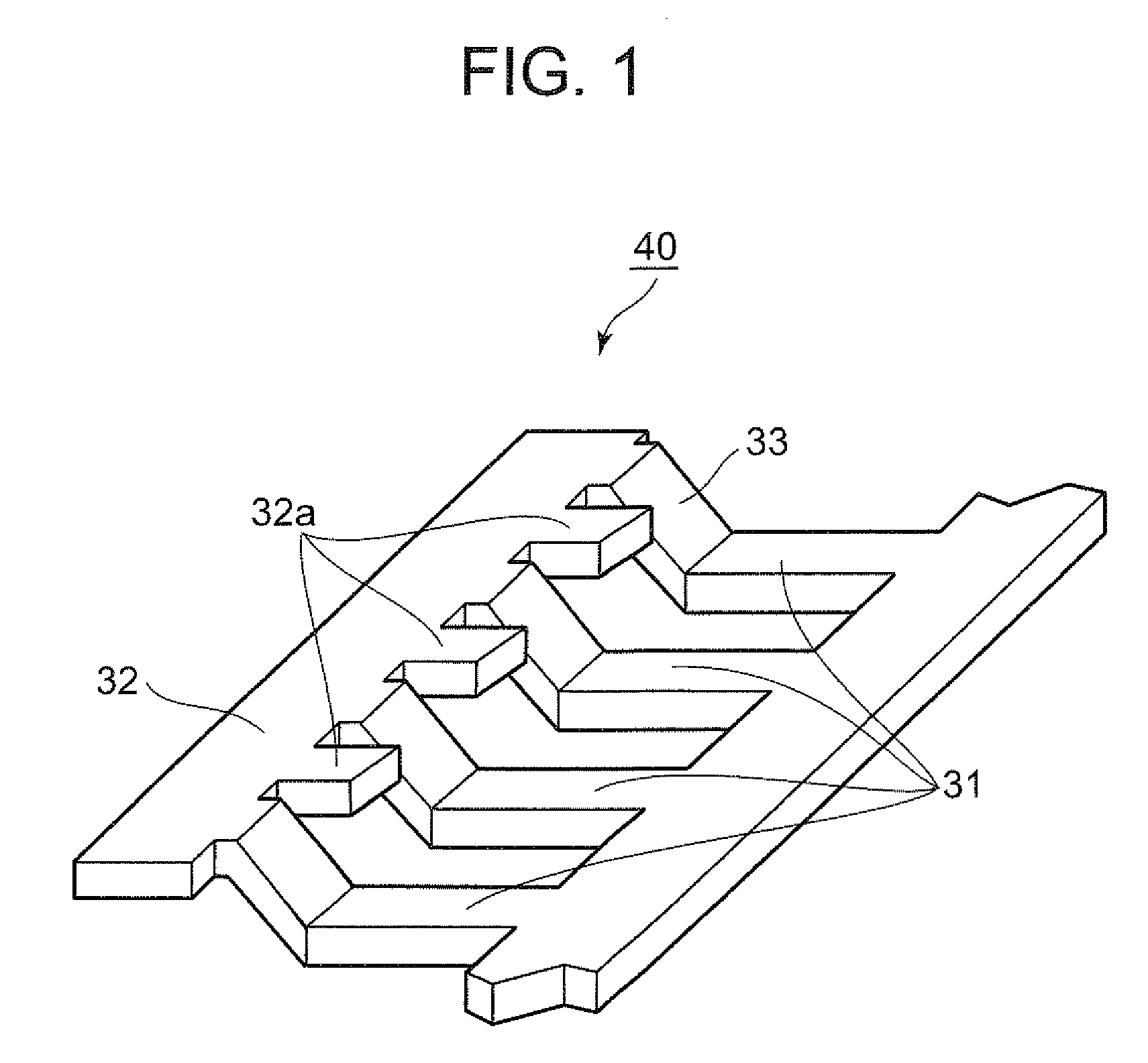
[0035]FIG. 1 is a fragmentary bird's eye view of the lead frame 40 in the first embodiment of this invention. This lead frame 40 includes an inner lead 32 depressed upwards from the outer lead 31. Namely, a step difference section (depressed section) 33 is formed between the outer lead 31 and the inner lead 32. A section of the inner lead 32 Includes a plurality of extended sections 32a extending towards the outer lead 31 side. The extended section 32a is provided to be adjacent to the step difference section 33. Forming the extended section 32a between two of the step difference sections 33 is advantageous. Forming this extended section 32a allows re...


PUM


Abstract

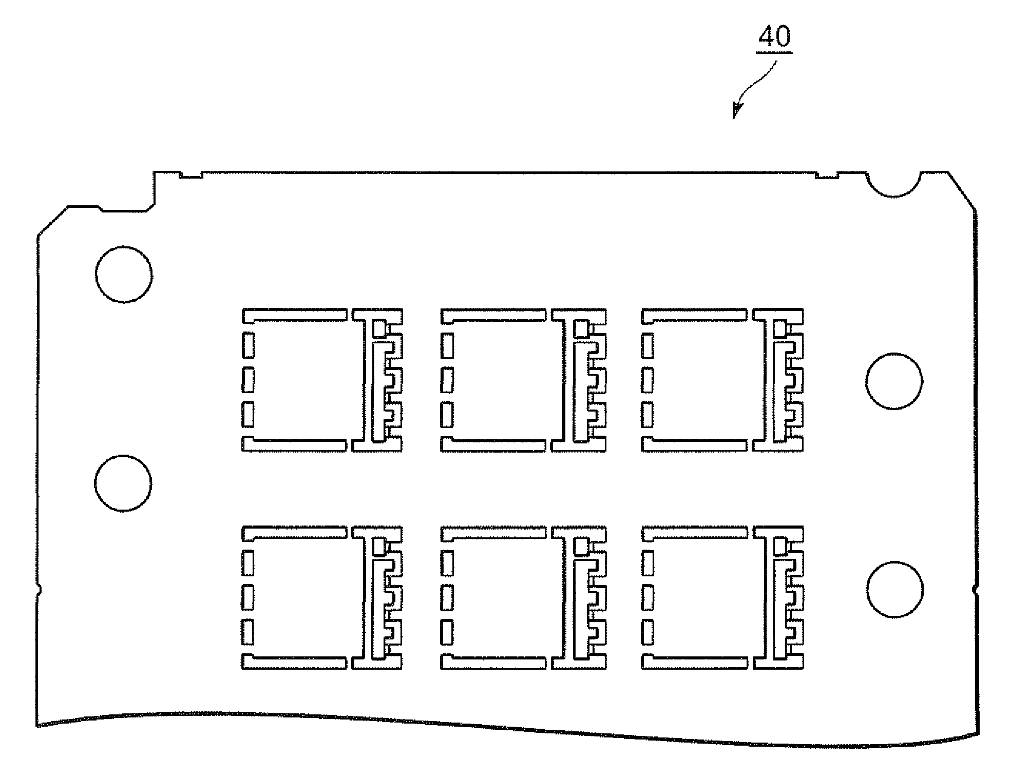
A lead frame and semiconductor device providing improved bond strength from wave bonding such as of wires in lead frames manufactured with depressed inner leads. The lead frame comprises an outer lead, an inner lead, a step difference section formed between the outer lead and inner lead, and an extended section extending from the inner lead towards the outer lead side. The extended section is provided to be adjacent to the step difference section. An acceptor clamp jig set on the lead frame includes a body, an inner lead support section and extended section support section respectively corresponding to the outer lead, the inner lead and the extended section. The outer lead is pressed from above by a retainer clamp jig. The extended section of the inner lead and the extension support section of the acceptor clamp jig prevent the tip of the inner lead from floating upward by acting together to accept and resist the tensile stress applied on the step difference section of the lead. Ultrasonic waves are in this way applied more efficiently and ultrasonic wave loss in the bond part between the inner lead and the wire is reduced.

Description

CROSS-REFERENCE TO RELATED APPLICATIONS[0001]The application is based upon, claims the benefit of priority of, and incorporates by reference the contents of Japanese Patent Application No. 2008-140850 filed on May 29, 2008.BACKGROUND[0002]1. Field of the Invention[0003]The present invention relates to a lead frame and a semiconductor device, and relates in particular to a lead frame possessing improved joint strength for ultrasonic wave bonding and a semiconductor utilizing that lead frame.[0004]2. Description of Related Art[0005]The lead frame utilized for manufacturing semiconductor devices is sometimes formed with a difference in height between the island and inner lead by forming the leads in a depress state with the aim of easily connecting the inner leads and the surface electrodes of the semiconductor chip with bonding wire and preventing problems such edge-touching of the wires.[0006]FIG. 6 is a schematic perspective view of the semiconductor device shown in FIG. 1 of Japane...

Claims


Application Information

Patent Timeline
IPC IPC(8): H01L23/495H01L21/50
CPCH01L23/49551H01L23/49562H01L2924/01033H01L2924/01006H01L2924/00014H01L2924/01082H01L2924/01005H01L2924/01004H01L2224/85205H01L2224/78703H01L2224/49111H01L2224/49051H01L2224/4903H01L2224/48472H01L2224/48247H01L2224/48091H01L24/85H01L24/49H01L24/48H01L2224/78H01L2924/00H01L2924/12033H01L2924/181H01L2224/45099H01L2224/05599H01L2924/00012
Inventor OKISHIMA, KAZUHIKO
Owner RENESAS ELECTRONICS CORP
Learn More